Mission and efforts of NTT Photonics Laboratories in support of optical communications technology
–What is the mission of NTT Photonics Laboratories?
As a set of laboratories under the umbrella of the NTT Science and Core Technology Laboratory Group, the NTT Photonics Laboratories researches and develops optical and electronic components and modules and new materials to drive technical innovation with the mission of expanding the information-communications business and opening up new business areas. In addition to researching and developing photonic devices to provide advanced and cost-efficient optical communications networks for the NTT Group, we are also researching devices that will become the key elements of future ubiquitous broadband networks five and ten years down the road.
–To begin with, what kind of technology is optical communications?
The concept of optical communications first appeared in the 1970s, almost 40 years ago. It got its start from the idea that a large volume of data could perhaps be conveyed through the use of a laser, which was invented in the 1960s. At that time, the passing of optical signals through a narrow glass fiber and their transmission to locations as far away as several hundred kilometers was only a dream. But over the years, great improvements in optical fiber and a significant decrease in optical loss within the fiber have made optical communications technology applicable to even submarine cables.
Despite these great advances in optical communications, we are not yet at the stage where optical signals can be used throughout the entire transmission path from the originator to the other party. In the present network, optical signals must be converted to electrical signals whenever signal processing is necessary. One day, we hope to be able to transmit optical signals without any conversion to electrical signals, but at present, it is still very difficult.
When thinking about optical signals, we can treat time as being, in one sense, equivalent to distance traveled. Then memory, the recording medium of electronic devices, corresponds to something that stops light. However, since light has no mass, this basically means that it cannot be stopped. In short, while light is useful for carrying information over long distances, it is not conducive to the construction of memory. It is for this reason that we cannot help but depend on electrons. It is difficult, however, to make electrons travel at high speed, and electrons slow down when they collide with atoms. In a sense, electrons and light have opposite properties, and in optical communications technology, this calls for systems that can exploit the good properties of both.
–With many optical communications technologies now being researched and developed at Photonics Laboratories, how are you addressing the most important research themes?
Key research at the Photonics Laboratories can be divided into three areas. The first is the field of optical semiconductors, where we research semiconductor lasers, the source of light in optical communications, and optical modulators and photodetectors, which act as intermediary devices between light and electricity. An optical modulator converts electrical signals to optical signals and a photodetector does the opposite.
The second area is optical glass technology. The core of this technology is the silica-based planar lightwave circuit (PLC), which was born from a convergence of optical-fiber fabrication technology developed at Photonics Laboratories and LSI (large-scale integration) fine-processing technology. A PLC is an optical integrated circuit that can integrate many functional elements on a planar substrate. In PLC technology, high-precision fabrication techniques result in high compatibility with circuit design rules and the ability to control the properties of light waves such as interference. In this way, we have been able to use PLCs in a wide range of functions including optical switches and optical splitters.
The third area is ultrahigh-speed electron devices. For us to achieve ultrahigh-speed optical communications, the electron devices performing electrical signal processing must be capable of high speeds. We are researching and developing key ICs (integrated circuits) and modules for the next-generation network, making use of compound-semiconductor electron-device IC technology. This technology uses materials like indium phosphide (InP) and gallium nitride (GaN), which have superb high-speed and high-frequency properties, in the place of silicon (Si), the most commonly used semiconductor material at present. However, raising the speed of electron devices increases the amount of power that they consume, and low-power design technology is an important research theme.
In this way, Photonics Laboratories possesses a variety of key technologies for optical technologies, and we develop photonic-device technologies through composite technologies that integrate these key technologies. In each of these research areas, we apply a range of fundamental and practical technologies, from materials technologies such as crystal growth methods that underlie all devices, to device-design and fine-processing technologies, measurement and evaluation technologies, and module packaging technology. Among these, device-design technology is the heart of optical communication devices. To achieve an excellent product with distinguishing features compared with outside products, it is important to determine at the design stage how a high-speed, low-cost, and low-power device is to be constructed while incorporating necessary functions.
Photonic devices and modules developed at Photonics Laboratories are evaluated in-house before being provided to other NTT laboratories such as Network Innovation Laboratories and Access Network Service Systems Laboratories. Comprehensive evaluations are then performed to determine whether certain devices and modules can actually be incorporated and used in a particular optical-communications system.
Coping with rapid change and reducing costs
–Optical communications technology is one of the fastest changing fields in the industry. How do you cope with rapid change?
Research on devices associated with optical communications began almost 40 years ago, and one way of looking at the field is that it took a sequence of achievements during that time to get us to where we are now. There are many products now in use that began to be researched about 10 years ago. In other words, it takes a relatively long time before a product can actually be put on the market once we decide that we need it. But misreading the direction of the market can mean a complete loss to the competition. Even when a company is one step ahead, inattention to the market can mean losing the lead in no time at all.
Device and component research is, of course, a universal endeavor with the result that device and component prices tend to fall as far as possible. From the customer's point of view, the only thing of concern is how low a product that fits his or her needs can drop in price. But at the same time, the products that we provide must be highly reliable and durable.
Take, for example, semiconductor lasers. Customers may desire certain functionalities such as a freely changeable wavelength or adjustable bit rate, but they also want a low price. From our side, we must, of course, shorten the time from research to product delivery while figuring out how to beat the competition and meet the above customer needs. These are all major issues.
–Can you name some products that have made it to the market by commercializing research results?
A number of our research achievements have made it to market. For example, PLC-related products such as optical splitters have been deployed in great number in NTT Group networks. The tunable laser array (TLA) is a recent example of research that has become practical (Photo 1). This device, in which the oscillating wavelength can be changed, is expected to be used as a light source in wavelength-division-multiplexing (WDM) systems that transmit optical signals of various wavelengths through a single optical fiber. At the Photonics Laboratories, we have made a TLA by integrating multiple semiconductor lasers of different oscillating wavelengths plus a coupler for bundling optical signals and an optical amplifier for amplifying optical signals on a single semiconductor chip. Although the variable wavelength width of an individual semiconductor laser is small, integrating many lasers with slightly different oscillating wavelengths achieves, in effect, a large variable wavelength width. This TLA is already being sold by companies in the NTT Group.
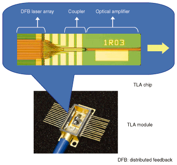
Photo 1. Tunable laser array (TLA).
The need for marketing-oriented R&D
–Dr. Yumoto, what is your particular concern about optical communications technology from here on?
At present, technology is progressing rapidly wherever you look. A company can easily fall behind the competition if it concerns itself only with what to do with the technology it currently possesses. The key to avoiding this scenario and succeeding is to observe and evaluate the outside world and the market. To this end, we must learn what the market demands and what the customer is thinking. One way of doing this is to have young researchers collect information on the overseas market through overseas training in the USA, for example. To begin with, we are working to train researchers to think in terms of the market. I think that the fate of optical-component development is a long R&D time with severe competition. To survive and expand under these circumstances, we must give special attention to the speed of R&D and the marketing of developed products.
↑ TOP