|
|||||||||||||||||||||||||
|
|
|||||||||||||||||||||||||
       |
Vol. 5, No. 9, pp. 12–19, Sept. 2007. https://doi.org/10.53829/ntr200709sp2 Optical Beam Scanner Using Kerr Effect and Space-charge-controlled Electrical Conduction in KTa1−xNbxO3 CrystalAbstractLarge angle, low-voltage electro-optic beam scanning has been achieved using KTa1−xNbxO3 crystal. An unprecedented deflection angle of 250 mrad (=14.3°) has been achieved by applying only ±250 V to a 0.5-mm-thick KTa1−xNbxO3 crystal with a short interaction length of 5.0 mm. The operating principle was investigated and the origin of the deflection phenomenon was attributed to a nonuniform electric field induced by space-charge-controlled electrical conduction in the crystal. This novel effect has been called the "space-charge-controlled EO effect". 
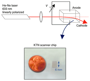
1. IntroductionOptical beam scanners are used in various application fields including printing, displays, sensing, and telecommunications. Electro-optic (EO) scanners have the attractive features of a rapid response and an arbitrary deflection angle compared with other technologies such as galvanic mirrors, polygon mirrors, microelectromechanical systems (MEMS) mirrors, and acousto-optic scanners. EO scanners refract optical beams by introducing a linear phase delay across the beam cross-section. The deflection angle is varied by electro-optically controlling the amount of the phase delay. A linear phase delay is commonly produced by forming an EO crystal [1], an electrode [2], or a ferroelectric domain [3] into a prism shape. To make an ultrafast EO scanner, a linearly graded refractive index is induced by a linear distribution of the modulation index with appropriately designed electrodes [4]. Besides these techniques, it is also possible to induce a linear phase delay with a nonuniform electric field in an EO crystal. In this case, a linearly graded refractive index is induced by the EO effect and the beam is cumulatively refracted as it propagates through the crystal. Fowler et al. demonstrated this method by using a quadrupole configuration of suitably designed electrodes with KH2PO4 [5]. However, in spite of the advantages of EO scanners and the continuous efforts made in device development, the high electric field needed to obtain a useful deflection angle has limited the practical use of conventional EO scanners. In this paper, I describe observations that my coworkers and I made of anomalous beam deflection in an EO crystal KTa1−xNbxO3 (potassium tantalate niobate, KTN) having a simple rectangular shape and a uniform electrode on its surface. KTN, which is a ferroelectric material, exhibits a large EO effect around the paraelectric-to-ferroelectric phase transition temperature Tc [1], [6], [7]. Our KTN scanner exhibited a very wide deflection angle of ±125 mrad (±7.16°) with a low electric field of ±500 V/mm and a short interaction length of 5.0 mm. This performance is unprecedented for an EO beam scanner and the deflection angle is wide enough for various practical applications. We propose that the origin of the anomalous beam deflection is the nonuniform electric field generated by the space-charge-controlled mode of electrical conduction in the crystal, which induces a linearly graded refractive index as a result of the EO effect. 2. KTN beam scanner2.1 SetupOur experimental setup is shown in Fig. 1. The crystal composition was adjusted to x=0.4, which yielded a Tc of about 35°C. The crystal temperature was kept at 5°C above Tc throughout the experiment to obtain a large EO effect. At this temperature, the crystal was in the paraelectric phase and the lowest-order EO effect was the quadratic Kerr effect. The Kerr constant s11 at this temperature was 1.0 × 10⁻¹⁴ m2/V2. The crystal was cut and polished to a rectangular shape 6 mm long and 0.5 mm thick. A key element of the deflection phenomenon is the formation of an ohmic contact between the electrodes and the KTN crystal to produce a space-charge-controlled mode of electrical conduction. This is discussed in section 2.2. A uniform titanium electrode (length L = 5 mm) was deposited on both surfaces of the crystal. The light source was a linearly polarized He-Ne laser (λ = 638 nm), and the polarization was aligned with the electric field.
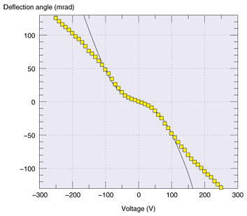
2.2 Beam scanning characteristicsThe experimental results for deflection angle versus applied voltage are shown in Fig. 2. When the voltage was changed from −250 to +250 V, the deflection angle changed from +125 to −125 mrad. The largest deflection angle for an EO scanner reported to date [3] is ±127 mrad obtained with a domain-engineered multiprism formed in LiTaO3 with an applied electric field of ±14,200 V/mm and an interaction length of 15 mm. The KTN scanner achieved almost the same deflection angle with an electric field of only ±500 V/mm and a short interaction length of 5 mm. Moreover, the KTN scanner has a simple rectangular shape and uniform electrodes. When we first observed this deflection phenomenon, we suspected that it resulted from either a nonuniform temperature distribution or the gradient of the crystal composition over the thickness of the crystal because we expected these conditions to induce a nonuniform refractive index. However, neither of these assumptions explained the phenomenon. We placed the crystal between large copper blocks, i.e., a heat reservoir, to ensure that we maintained a uniform temperature, but the deflection angle did not change. And if the deflection had been the result of the gradient of the crystal composition, the sign of the deflection angle would have been reversed by placing the crystal upside down, but the deflection angle remained unchanged. We also checked the parallelism of the incident and output facets. The measured value was better than 5 mrad, which is too small for such a large deflection to be explained by the prism effect. We then considered the electrical characteristics.
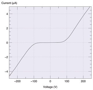
The I-V characteristics of the KTN crystal are shown in Fig. 3. They exhibit an unexpected feature, namely a linear-to-nonlinear transition with a transition voltage of about 40 V. This distinct feature reminded us of space-charge-controlled (or space-charge-limited) electrical conduction in solids. An important feature of the space-charge-controlled mode is that the electric field becomes nonuniform between the anode and cathode. In the space-charge-controlled mode, electrical conduction is dominated by injected charges rather than by thermally excited free charges. The departure from Ohm's law to nonlinear I-V characteristics is a strong manifestation of the space-charge-controlled mode. An underlying assumption for the space-charge-controlled mode is that the contact between the electrode and the crystal is ohmic so that the charges are sufficiently injected into the crystal. After investigating the electrical contact of different materials with KTN, we found that a titanium electrode forms an ohmic contact for electron conduction in the KTN, so we used this electrode material in our experiment. For comparison, when we used a Schottky contact, which was found to be formed with a platinum electrode, no significant departure from Ohm's law was observed and the beam was not deflected. Platinum has a larger work function than titanium, so it creates a higher energy barrier at the contact. This result also supports the proposal that the deflection phenomenon originates from a nonuniform electric field induced by space-charge-controlled electrical conduction.
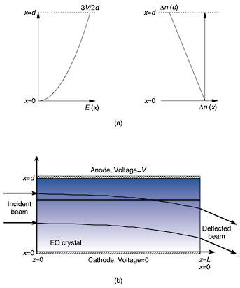
3. Principle of operation of beam scanning phenomenon3.1 Theoretical analysisEO crystals are generally considered to be insulators because they are dielectric materials and ideally do not have conduction electrons. However, if the contact between the electrode and the crystal is ohmic and electrons are injected into the conduction band of the EO crystal, then electrical conduction by electric field drift and/or diffusion is possible. The space-charge effect manifests with such collective motion of injected electrons. Since the injected electrons exist as true charges in the crystal, they terminate the electric field originating from the anode [8]. Below, we formulate the distribution of the electric field, refractive index change induced by the Kerr effect, and the beam propagation in the crystal. The governing equations are those of Gauss's law and the current continuity law, which relate the E-field to the density and motion of the injected electrons. The electric field E(x) and the injected electron density N(x) are related by Gauss's law as follows:
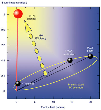
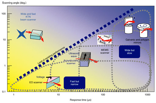
As the optical beam propagates through crystal, it is refracted by the linearly graded refractive index, which is schematically shown by the color gradation in Fig. 4(b). For a paraxial beam, the deflection angle θ external to the crystal after the beam has traveled a distance equal to the interaction length L is given by 4. Scanner applicationEO beam scanners generally have attractive features such as a high-speed response and digital/analog scanning capability. However, the high voltage required to achieve a reasonable angle has been limiting their use in practical applications. The performance of previously reported EO beam scanners is summarized in Fig. 5 [1]–[3]. For the LiTaO3 multiprism scanner, which contained 10 prisms in a device length of 15 mm, the scanning angle was normalized to a device length of 5.0 mm to enable us to compare its performance with that of the KTN beam scanner. The KTN scanner is more efficient than the other EO scanners by almost two orders of magnitude. Our KTN scanner is even more efficient than the prism-type KTN scanner. Moreover, when the KTN scanner is compared with moving mirrors such as polygon and galvanic mirrors, which are widely used in laser printers, photocopiers, and so on, we see that its response time is 100 times better and that the device volume can be 1/100 as large while achieving a comparable scanning angle [9], as shown in Fig. 6.
Another performance criterion of the optical beam scanner is the number of resolvable spots, which is defined by the full scan angle divided by the full angle of the beam divergence. In the experiment, even though the crystal thickness was 500 μm, we had to focus the beam to 80 μm (1/e2 diameter) to avoid any unwanted diffraction resulting from residual fluctuation of the Ta/Nb ratio in the crystal. The number of resolvable spots was about 20 with this limited beam diameter. We are now successfully improving the crystal growth technique to reduce the fluctuation, and we expect the number of resolvable spots to be about 80 for a Gaussian beam input with 1/e2 diameter of 260 μm provided that we can utilize the full aperture of the crystal. The number of resolvable spots increases in proportional to the aperture size. There is a trade-off between the number of resolvable spots and the applied voltage because the beam deflection is parallel to the electric field rather than perpendicular to it as in the prism-type scanner. 5. ConclusionOur EO beam scanner achieves unprecedented performance through the space-charge-controlled EO effect in KTN crystal. We propose that the operating principle is based on the space-charge-controlled mode of electrical conduction and the Kerr effect. This seems to offer a good explanation of the deflection phenomenon. The deflection phenomenon has been consistently observed with KTN crystals with different crystal compositions grown in our laboratory. The Tc for these KTN crystals ranges from −40 to +120°C. We are now undertaking a detailed investigation of such deflection phenomenon and an exact theoretical analysis. The KTN scanner is expected to be used not only in optical communications, but also in printing, imaging, displays, and other applications. References
|
||||||||||||||||||||||||