|
|
|
|
|
       |
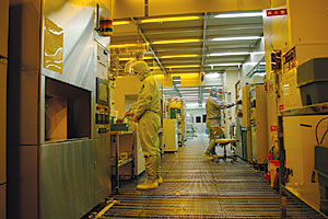
Spotlight on NTT Laboratories Vol. 5, No. 10, pp. 1–5, Oct. 2007. https://doi.org/10.53829/ntr200710lab  R&D of Advanced Hardware Technology for the Creation of Ubiquitous ServicesAbstractIn this issue, we turn the spotlight on NTT Microsystem Integration Laboratories, which is located at the NTT Atsugi R&D Center in Kanagawa prefecture. In addition to new communications technologies, these laboratories research and develop advanced electronics and sensor technologies as platform technologies for the coming ubiquitous era. To learn more about core R&D and high-profile technologies at Microsystem Integration Laboratories, we talked to General Manager Hakaru Kyuragi, who oversees more than 100 employees.  Role of Microsystem Integration Laboratories at NTT—Dr. Kyuragi, the laboratories you manage undertake R&D essential for the ubiquitous era. How is Microsystem Integration Laboratories positioned within NTT Laboratories and what role does it play? NTT Laboratories is divided into three main laboratory groups: the Cyber Communications Laboratory Group, Information Sharing Laboratory Group, and Science and Core Technology Laboratory Group. Of these, the Science and Core Technology Laboratory Group consists of three platform research laboratories and two basic research laboratories. We are one of those platform research laboratories with the role of researching and developing hardware technology for ubiquitous systems. Specifically, we research network-oriented LSIs (large-scale integrated circuits) as the foundation for advanced electronics technologies plus a variety of sensors and other products to support safe and secure living, especially in medical care, food inspection, and structural diagnosis of buildings. These hardware devices are indispensable for the ubiquitous era, but as opposed to being directly visible to users as in the case of cell-phones, they tend to function as an intermediary between the user and advanced technology in a “behind the scenes” manner. Grouping R&D into three priority areas—What R&D fields are your researchers putting most of their efforts into? At present, Microsystem Integration Laboratories is grouping its research themes into three priority areas: system LSIs for telecommunication network use, spatial-optical communication devices, and sensors and appliances for ubiquitous services. In doing so, we aim to simplify the setting of specific R&D targets, allocate management resources in a systematic and effective manner, and plan for high-impact research results. First, in the area of system LSIs for telecommunication network use, we are researching their elemental devices in preparation for business in the near future. We are currently using GE-PON (gigabit Ethernet passive optical network) as the technology for delivering optical communication services to customer households at a bit rate of 1 Gbit/s. For the future, there are moves in standardization bodies to increase this to 10 Gbit/s. We are therefore moving forward on the development of high-speed LSIs for optical communications as a base technology for processing ultrahigh-speed signals. In this research, we are collaborating with NTT Photonics Laboratories and NTT Access Network Service Systems Laboratories. Second, in the area of spatial-optical subsystems, research into 3D-MEMS (three-dimensional micro-electromechanical systems) optical switches is becoming a major pillar of our work. The spread of broadband services has led to a dramatic increase in network traffic, and one key product on the network side for handling this traffic is a three-dimensional optical switch that can control optical signals using MEMS mirrors. In this technology, however, optical signals travel through space, which means there are more degrees of freedom, so signal control is more difficult. To solve this problem, we are working to develop compact but large-scale multichannel switching exploiting the features of three-dimensional space (Photo 1).
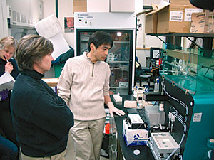
Third, in the area of sensors and appliances for ubiquitous services, Microsystem Integration Laboratories looks to create ubiquitous services to provide novel communication tools and new lifestyles. We aim, in particular, to lead the way to a genuine ubiquitous society using new communication technologies and diverse sensor technologies. In our present research, we have developed technology for a 10-Gbit/s high-speed radio link using ultrahigh-frequencies in the 120-GHz millimeter-wave band. —What technologies have been commercialized? With regard to the above three areas of R&D, one great example of a commercialized technology is our one-chip fingerprint identification technology. Existing fingerprint identification systems first detect a fingerprint using a sensor and then identify it with a processor. This means that a fingerprint identification system can be implemented only by expensive electronic instruments. In contrast, our fingerprint LSI incorporates all functions—from the registering of fingerprint data to the matching and identification of input data against registered data—on a single chip (11 mm × 15 mm × 1 mm) that integrates the sensor and processor. This device has made it possible to apply a fingerprint identification system to compact portable products and inexpensive electronic devices that can act as biometric keys. New core technologies for ubiquitous broadband services—It appears that Microsystem Integration Laboratories is focusing much attention on new and unique communication technologies. Absolutely. For example, RedTacton is a technology that provides the user with a new communication tool. Its name comes from the combination of the words “red” (referring to warmth), “contact,” and “action.” Combining the feature of conventional communications, whereby a wired connection is essential for two parties to communicate, with the property of portability in wireless communications, RedTacton can convey information using an electric field transmitted over the surface of an object or a human body. It is a new communication tool for the ubiquitous society. —How will RedTacton make life more convenient for users and what application fields can be considered? Although increased security is essentially at odds with ease of use, this technology can achieve user-friendly operation while maintaining a high level of protection. This is because signals are conveyed over one's own body or over something attached to one's body, which means that there is no need to insert or remove media and no reason to worry about information being stolen without you realizing it, as in the case of wireless communications. With RedTacton, information is conveyed only via something that you touch. In short, information technology (IT) and information-communications technology (ICT) will become associated with intuitive and natural human actions. RedTacton can be seen as a technology suitable for personal use because it allows interaction through intuitive and natural human actions. It can transfer information identifying the user so that a door can be opened when you simply touch the door knob or user authentication can be performed when you just sit on a chair. It can be used, for example, in an office space designed for desk-sharing and flexible non-dedicated working arrangements, where there is no desire to construct partitions, but there is a need to identify specific persons. Because technology like RedTacton has a close relationship with market needs, we have set up a RedTacton demonstration room in our research laboratories to hear what customers have to say about this new technology, and we are holding field trials with collaborating companies to advance our research. Management must not crush new ideas—A research laboratory has many technology seeds, and hurdles and hardships must be overcome to develop and commercialize them. From a management viewpoint, what in particular do you think needs diligence? Executing something new requires new concepts and ideas, but we sometimes forget that researchers themselves might get trapped within their own value system. From the management side, it is my job to offer pertinent advice in the planning stage or during various processes. At the same time, if it is assumed that I do not give credence to the ideas of young researchers, I may be nipping new ideas in the bud. It is therefore imperative that I have a clear understanding of what researchers are saying and thinking. In the end, I must strike a balance between giving advice and suppressing my preconceived notions, so as not to crush fresh ideas. This is a difficult task. Researchers should not be satisfied with the status quo. Being satisfied with the range of knowledge that they or their research groups possess will only lead to stagnation. Competitors are working hard on the outside. They are always conscious of this, and for this reason, they need to set high targets for themselves and to strive to achieve their goals faster than anyone else. Importance of tying up with and collaborating with other companies—Technology is advancing, the services that use it are diversifying, and the competitive environment with the rest of the world is becoming severe. Against this background, what is it that you must keep in mind when engaged in R&D? In system creation, simply making components and devices will not lead to a product conducive to implementation. Within the processes of research, development, and commercialization, it is essential that we collaborate with NTT Group companies and other manufacturers even in the initial stage of development, and that we clearly delineate our roles and draw up a scenario for commercialization. Due consideration must also be given to the manufacturing system, post-sales follow-up, and maintenance. To arrive at R&D success, it is important that we set up a system for tying up with many concerned parties. In the end, this can help minimize design changes and losses and obtain R&D results in a relatively short period of time. This is not an issue affecting only Microsystem Integration Laboratories—it is common to all R&D. —What is your outlook for the future? We will continue with research and development in the priority fields that I described, with “high speed” and “low power consumption” being keywords in our work. From the beginning, Atsugi R&D Center's core competence has been high-speed ICs (integrated circuits) and low-power LSIs. Making use of this technical expertise, I would like us to undertake the research and development of sensors that operate on an extremely small amount of energy or that incorporate natural energy, eliminating the need to replace batteries, and of environment-friendly components and devices. Short profile of Microsystem Integration LaboratoriesFrom the outside, this set of laboratories is difficult to learn about. Here, we introduce some of its activities. Joint researchThe University of Wisconsin at Madison in the United States is a destination for long-term stays by researchers at Microsystem Integration Laboratories. It is here that joint research on biosensors is being conducted (Photo 2). The state of Wisconsin lies between Lake Michigan and Lake Superior (two of the five Great Lakes) in a region with abundant dairy farms.
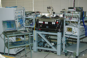
LSI measuring equipmentThis equipment is used to evaluate advanced LSIs designed at Microsystem Integration Laboratories (Photo 3).
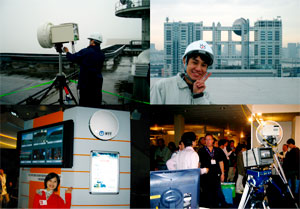
Joint trials of 120-GHz millimeter radio technologyJoint trials on ultra-broadband radio communications using electro-optical technologies are in progress (Photo 4). This technology enables the simultaneous transmission of up to six channels of uncompressed HDTV signals.
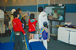
High-reality 3D capture systemChildren enjoy virtual experiences using automatically generated 3D computer graphics (Photo 5). This technology can be applied to various types of simulations and product and service promotions.
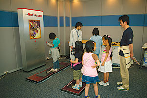
An especially busy day at Atsugi R&D CenterA special feature here at the Atsugi R&D Center and Microsystem Integration Laboratories is the Atsugi R&D Center Open House held annually in April. On this day, the laboratories are open to the public, including a great number of families with children. Every year, Microsystem Integration Laboratories sets up a hands-on corner aimed at elementary-school students based on a certain arrangement of research results. This year's attraction—entitled “Kids Technology Playland”—was designed so that whole families could participate. Needless to say, specialized terminology was of no use on this day, and research staff in charge of explaining the technology found themselves struggling to answer unexpected questions from many children. A hands-on display of RedTacton technology is shown in Photo 6. Here, children were able to experience the act of communicating by performing natural human actions like stepping or touching. This display enabled the children to experience for themselves cutting-edge communication technology ahead of its time.
In a speech given by Hakaru Kyuragi, General Manager of NTT Microsystem Integration Laboratories, he said that “Informing local residents of the work that we are doing at Atsugi R&D Center through activities like this is an important part of our mission. If this open house can generate even a little interest in advanced technology in children, perhaps some of them will one day continue in our footsteps as researchers.” The Atsugi R&D Center open house is actually becoming a seasonal tradition in the Atsugi City area. |