|
|||||||||||||||||||||||||
|
|
|||||||||||||||||||||||||
       |
Selected Papers: MEMS Device Technologies Vol. 5, No. 10, pp. 11–16, Oct. 2007. https://doi.org/10.53829/ntr200710sp2 Electrodeposition of Organic Dielectric Film on MEMS Devices for Improved ReliabilityAbstractThis paper introduces a technique that prevents sticking between an actuator and a control electrode during the operation of a microelectromechanical systems (MEMS) device. It involves the electro-deposition of an organic dielectric film on the gold electrode. In a vibrating MEMS device pretreated by hydrochloric acid dipping, the electrodeposited film exhibited an excellent anti-sticking effect between the vibrator and the electrode. This will ensure high durability for such devices. 
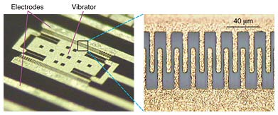
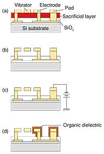
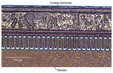
1. IntroductionMicroelectromechanical systems (MEMS) technology is attracting a great deal of interest as a way to fabricate movable microstructures (actuators) on a silicon substrate [1]. The actuators are fabricated by the release ashing of a thin film (sacrificial layer) beneath their microstructures. A common way of making an actuator move is to apply a voltage to produce an attractive electrostatic force between the actuator and an adjacent control electrode. In such MEMS devices, the actuator often sticks to the control electrode while the device is operating. That is, when the voltage is too large, the actuator can no longer be controlled and pull-in occurs. Then, an electrical resistance weld forms, which causes the actuator to stick permanently to the electrode and no further movement is possible. This is called in-use sticking. It can also cause an electrical short. Therefore, a major issue in fabricating MEMS devices is how to prevent sticking and electrical shorts. One good solution is to encapsulate the actuator and/or electrode with an organic dielectric film. In this paper, we describe the electrodeposition of an organic dielectric film on a gold electrode in a vibrating MEMS device consisting of a gold vibrator and electrodes, both of which have comb-shaped structures with a high tooth density [2], [3]. The electrodeposition technique prevents electrical shorts and in-use sticking between the gold vibrator and electrode, ensuring high durability. 2. Problem with electrodeposition after ashingWe applied the technique to the gold electrode in a vibrating MEMS device (Fig. 1), where the photograph on the right is a magnified view of an area around a gold vibrator and an electrode both having comb-shaped structures with a high tooth density [2], [3]. The electrodeposition procedure is shown in Fig. 2. After the wafer had been diced into chips (Fig. 2(a)) and the vibrator on a chip had been released by oxygen plasma exposure for sacrificial-layer ashing (Fig. 2(b)), the chip was immersed in the solution. The source materials were sulfonium cations with epoxy groups (INSULEED 3020; Nippon Paint) [4]. Then, a negative voltage of -7 V was applied to only the gold comb-shaped electrode through a pad for 15 s at a solution temperature of 30°C (Fig. 2(c)). Finally, the chip was annealed in a nitrogen ambient to evaporate the solvent and harden the film (Fig. 2(d)).
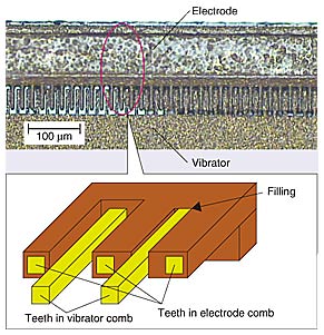
An optical microscope image of an area near the electrodeposited gold comb-shaped electrode is shown in Fig. 3. Uniform growth would have resulted in the deposition of a 0.5-µm-thick film on the electrode, but the thickness of the deposited film after the release ashing process was not uniform. Moreover, some of the gaps between the comb teeth were completely filled. This prevented the vibrator from moving freely.
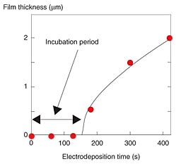
To determine the cause of the nonuniformity in the deposited film, we analyzed the front and back surfaces of the gold comb-shaped vibrator. We found that oxidation occurred during the release ashing of all the gold surfaces and that the amounts of gold oxide were different at different places. To clarify what was happening in the electrodeposition on such gold surfaces exposed to oxygen plasma, we examined the characteristics of deposition on evaporated gold surfaces after oxygen plasma exposure. The organic dielectric film was deposited at an applied voltage of -7 V at a solution temperature of 30°C. The relationship between the thickness of the annealed film and electrodeposition time is shown in Fig. 4. In electrodeposition on the oxidized gold surface, an incubation period, during which the film did not grow, was observed in the initial stage. After the incubation, the film grew rapidly. Any slight difference in the length of the incubation period could therefore lead to a big nonuniformity in film thickness.
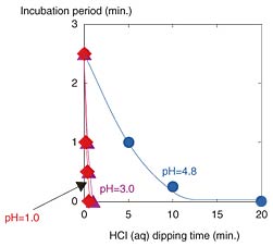
We have previously confirmed that there was no oxygen at the interface between the gold surface and the deposited film, which indicates that the gold oxide disappears after deposition [5]. This suggests that the incubation period is the time needed to remove the gold oxide formed during oxygen plasma exposure. This means that the incubation proceeds nonuniformly, because there are different amounts of gold oxide at different places, and thus produces variations in the thickness of the deposited film. This explains the nonuniformity in film thickness shown in Fig. 3. 3. Elimination of incubationTo eliminate the incubation, we examined hydrochloric acid (HCl(aq)) dipping because Au2O3 is the only gold oxide known to be soluble in HCl(aq) [6]. We applied HCl(aq) treatment to evaporated gold surfaces exposed to oxygen plasma at an RF (radio frequency) power of 100 W for 6 min. Figure 5 shows the relationship between the length of the incubation period in this most strongly oxidized surface and dipping time with the pH of HCl(aq) as a parameter. Electrodeposition was performed at an applied voltage of -7 V at a solution temperature of 30°C. As dipping time increased, the incubation period decreased. Moreover, as the pH of HCl(aq) dropped from 4.8 to 1.0, the time needed to eliminate the incubation period decreased markedly from 20 min. to 30 s. These results show that HCl(aq) dipping can completely eliminate the incubation, which means that even gold oxide with different chemical states will be removed by dipping in HCl(aq).
4. Application to vibrating MEMS devicesThe uniform-electrodeposition technique with an HCl(aq) dipping pretreatment was applied to vibrating MEMS devices after release ashing. Figure 6 shows an optical microscope image of an area near the coated gold comb-shaped electrode in a vibrating MEMS device that had been dipped in HCl(aq) with a pH of 3.0. The electrodeposition was carried out under the conditions described in Section 2. The thickness of the annealed film was 0.5 µm with a variation of 10%. Note that, in contrast to the electrodeposition without HCl(aq) dipping (see Fig. 2), none of the gaps between the teeth in the gold comb-shaped electrode were filled. These results show that HCl(aq) dipping markedly reduced the degree of variation in film thickness.
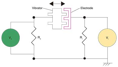
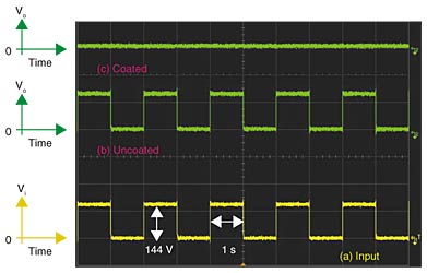
5. Prevention of electrical shorts and in-use stickingTo assess the effectiveness in preventing electrical shorts, we prepared two vibrating MEMS devices. For one, an organic dielectric film 0.5 µm thick was deposited on the gold comb-shaped electrode using the electrodeposition technique with the HCl(aq) dipping pretreatment. For the other, no film was deposited. Electrical response characteristics were observed with an electrical circuit (Fig. 7) to evaluate whether or not electrodeposition prevented electrical shorts. A 0.5-Hz 144-V rectangular signal ((a) in Fig. 8), which is 50% larger than the pull-in voltage of 96 V, was input between the vibrator and the control electrode to cause complete pull-in. For the device with the uncoated electrode, an output signal ((b) in Fig. 8) appeared every time there was an input signal. This means that electrical shorts occurred between the vibrator and the electrode for the uncoated device. On the other hand, for the device with the coated electrode, there was no output signal ((c) in Fig. 8), even when a voltage larger than the pull-in voltage was applied. This means that the organic film worked as an excellent insulator. These results demonstrate that an organic dielectric film prevents electrical shorts. In a durability test, we confirmed that the coated device still performed without any electrical shorts after ten million impacts between the vibrator and electrodes during vibration at a resonant frequency of 1.8 kHz. This shows that the deposited film has high reliability in that no electrical breakdown occurred during the repetitive operation at the applied voltage of 144 V.
In addition, we confirmed that the organic dielectric film prevents in-use sticking. For the uncoated device, the vibrator stuck to the control electrode during the first oscillation and did not become unstuck. On the other hand, for the coated device, there was no sticking, even when the vibrator came into contact with the electrode. We can therefore conclude that encapsulation by the electrodeposition technique with HCl(aq) dipping pretreatment prevents electrical shorts and in-use sticking between the gold vibrator and comb-shaped electrodes of vibrating MEMS devices, thus ensuring high durability. 6. ConclusionWe developed a technique for achieving uniform electrodeposition for complicated MEMS devices consisting of many pairs of a gold movable part and an electrode after release ashing. HCl(aq) dipping before electrodeposition completely eliminated incubation, thereby increasing the uniformity of the film thickness. We applied the electrodeposition technique with HCl(aq) dipping pretreatment to the fabrication of a gold comb-shaped electrode in a vibrating MEMS device and demonstrated that an organic dielectric film deposited by this technique prevented electrical shorts as well as in-use sticking. We observed neither electrical shorts nor in-use sticking after more than ten million impacts between the vibrator and the electrodes. This technique paves the way for improving the reliability of MEMS devices in practical use. References
|
||||||||||||||||||||||||