|
|||||||||||||||||||||||||||||||||
|
|
|||||||||||||||||||||||||||||||||
       |
Selected Papers: Forefront of Basic Research at NTT Basic Research Laboratories Vol. 6, No. 8, pp. 1–6, Aug. 2008. https://doi.org/10.53829/ntr200808sp1 Trapping and Delaying Light with an Ultrahigh-Q Photonic Crystal NanocavityAbstractWe have fabricated a photonic crystal (PhC) nanocavity based on a width-modulated line defect and investigated it in the time domain. The obtained quality factor (Q) was extremely high, 1.2×10⁶, which corresponds to a photon lifetime of 1 ns. The photon lifetime was directly measured in the time domain using the ring-down method—a technique that has the potential to provide detailed information about the temporal dynamics of PhC nanocavity systems. Indeed, we investigated the dynamic tuning of Q and the pulse transmission using a similar technique. In the pulse transmission experiment, the pulse exhibited ultraslow propagation with a group velocity of 5.8 km/s. The demonstration of slow light on a chip paves the way for the development of various quantum and classical integrated devices. 
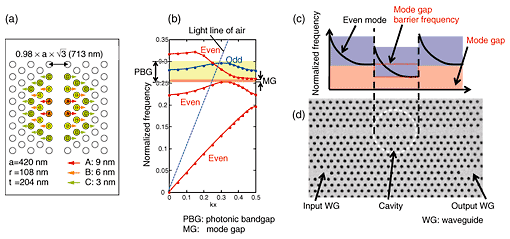
1. IntroductionUltrasmall cavities with ultrahigh quality factors (Q) have attracted great interest in recent years [1]. The Q is given by Q=ω0E/Pout , where ω0, E, and Pout are the resonant angular frequency, stored energy in the cavity, and power leaking from the cavity, respectively. Hence, a high-Q cavity can store a large amount of energy even with a low input power. High-Q nanocavities are attractive for achieving all-optical switching with ultralow energy [2], low-power optical bistability [3], or efficient cavity quantum electrodynamics [4], whose operations rely on a strong interaction between light and matter. Of the various micro- and nanocavities, photonic crystal (PhC) nanocavities are the smallest [5] and they enable us to fabricate compact photonic circuits on a chip. The speed of today's processors is limited by the speed of electronic devices because signal processing is performed electronically. All-optical signal processing has the advantage of a very high speed. In addition, if we treat data all-optically we can make use of the quantum nature of light, which may open up the possibility of developing devices with novel functions. The density of photons in a cavity scales with Q/V for a given input energy, where V is the mode volume of the nanocavity; hence, an ultrasmall cavity with an ultrahigh Q is attractive in terms of achieving a high photon density. Because an ultrahigh Q cavity will securely trap photons for a long time, the interaction between light and matter becomes effectively strong. However, it is not always easy to achieve a large Q/V because light travels very fast but is fundamentally difficult to stop or store in a small space. A PhC has an artificial dielectric structure, where the refractive index is periodically modulated on the scale of optical wavelengths. By analogy with an electrical property of materials (the presence of an electrical forbidden band), a PhC can have a photonic bandgap, where photons are not allowed to propagate. Since PhCs provide strong light confinement, they are ideal materials with which to fabricate small optical cavities. PhCs are often fabricated using a semiconductor slab, such as a silicon membrane, by patterning periodic air holes to produce what is called a two-dimensional (2D) PhC. The advantage of 2D PhCs is that they enable us to exploit sophisticated planar semiconductor process. Indeed, the highest Q for a PhC nanocavity has been achieved with a 2D silicon PhC because silicon fabrication technology is well developed. In this paper, we present results for the temporal dynamics of a width-modulated line-defect ultrahigh-Q PhC nanocavity fabricated on a 2D silicon PhC. The rest of this paper is organized as follows. First, we describe the structure of the width-modulated line-defect PhC nanocavity and explain the concept of light confinement. We present spectral measurement results that show that this cavity can yield an ultrahigh-Q of 1.2×10⁶. Next, we discuss a time-domain measurement based on the ring-down method, where we directly measured an extremely long photon lifetime of 1 ns. Finally, we report another time-domain study of an ultrahigh-Q nanocavity: the slow propagation of light. 2. Ultrahigh-Q PhC nanocavity2.1 Width-modulated line-defect PhC nanocavityFor 2D PhC nanocavities, it is important to find a structure that has a small out-of-slab radiation mode in order to achieve an ultrahigh Q. Various schemes for achieving an ultrahigh Q in a 2D PhC nanocavity have been studied. Among these, hexapole mode cavities and width-modulated line-defect PhC cavities have very small out-of-slab radiation and therefore a high Q. A hexapole mode cavity has a theoretical Q of 1.4×10⁶ and a value of 3.2×10⁵ has been experimentally measured, while the mode volume is extremely small, 1.18(λ/n)3 ≈ 0.11 µm3, where λ is the wavelength of light and n is the refractive index of the material (n=3.46 for silicon) [6]. A PhC nanocavity based on a width-modulated line defect has an even higher theoretical Q of >1×10⁸ and an experimental value of 1.3×10⁶, while the mode volume is 1.51(λ/n)3 ≈ 0.13 µm3 [7], [8]. The difference between the theoretical and experimental Q values arises from fabrication errors such as air-hole diameter and position fluctuations. The schematic structure of the width-modulated line defect PhC nanocavity is shown in Fig. 1(a). To achieve light confinement, the air holes at the cavity are slightly shifted away from the line defect. The shift is only a few nanometers. A photonic dispersion diagram of a PhC line defect with one row without holes, which helps us to understand the principle of light confinement, is shown in Fig. 1(b). The even mode exhibits low-loss light propagation in the line defect direction, but the odd mode is leaky. This graph reveals that no mode is present when the frequency is lower than 0.27, which is called the mode-gap region. The line defect is wider at the center, and this shifts the even (propagation) mode towards a lower frequency. As a result, a mode gap barrier is created, as shown by the dotted square region in the schematic illustration of Fig. 1(c). If we change the width of the line defect locally, we can confine the light (in the line-defect direction) with mode-gap barriers. In addition to horizontal confinement, it is known that the vertical radiation for mode-gap confinement is very small, which leads to an ultrahigh Q [9], [10]. A scanning electron microscope image of a fabricated PhC nanocavity coupled to input and output PhC waveguides is shown in Fig. 1(d). It was fabricated from a standard silicon-on-insulator wafer by using the conventional planar semiconductor process. The circled region is the cavity. Although it is difficult to recognize, the air holes at the cavity are slightly shifted towards the outside.
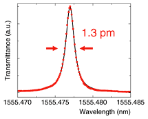
2.2 Spectral measurementThe measured transmittance spectrum of the fabricated sample is shown in Fig. 2. The spectral width is 1.3 pm, which corresponds to a Q of 1.2×10⁶. The measurement was performed by sweeping the wavelength of a tunable laser diode and recording the transmitted power. The input power was kept sufficiently low to prevent the cavity from exhibiting any nonlinearity that might modify the Q value. For such an extremely small spectral width, it is difficult to perform an accurate measurement. To obtain greater accuracy, we developed an alternative method for characterizing ultrahigh-Q cavities in the spectral domain, in which we used a single-sideband modulator to generate frequency-shifted light for sweeping the wavelength. By using multiple methods for the spectral measurement, we confirmed the ultrahigh Q and the accuracy of the measured results. Spectral measurement performed using a single-sideband modulator is described in detail elsewhere [11].
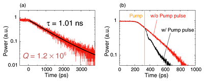
3. 1-ns pulse trapping in PhC nanocavityIt is well known that the photon lifetime τ of a Fabry-Pérot cavity can be obtained from the Q value, or vice versa, through the following equation: Q = ωτ (1) where ω is the angular frequency of the cavity resonance. A cavity with a Q of 1.2×10⁶ corresponds to a photon lifetime of 1 ns at the wavelengths used for telecommunications. Although the photon lifetime can be obtained from spectral measurements (i.e., by measuring the Q of a cavity), as shown with Eq. (1), it is important to measure the photon lifetime directly in the time domain. Time domain measurement enables us to discuss the dynamic behavior of PhC nanocavity systems. To obtain the photon lifetime in the time domain, we performed a ring-down measurement. We first injected continuous-wave laser light and then suddenly turned it off. By measuring the exponential decay signal from the cavity, we could directly obtain the photon lifetime. This kind of time-domain measurement is important for accurately characterizing the photon lifetime and because it enables us to obtain information about the nonlinear dynamics of the cavity system separately from that of the linear response. The measured ring-down waveform from a PhC nanocavity with a Q of 1.2×10⁶ is shown in Fig. 3(a). The output waveform exhibits a smooth exponential decay with a lifetime of 1.01 ns. The corresponding Q is 1.2×10⁶, which agrees perfectly with that obtained from the spectral-domain measurement. This is a direct demonstration of long-term photon caging in a small (wavelength-scale) cavity. It should be noted that light propagates 0.3 m in 1 ns in a vacuum, and this demonstration showed that the photons were trapped in a very tiny volume of 0.13 µm3 for the same period of time. The challenging part of this measurement was that we needed to use a very low-input laser light and record a weak output to prevent the cavity exhibiting nonlinearity such as two-photon absorption. To perform sensitive measurements, we used a time-correlated single photon counter.
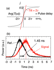
As discussed above, time domain measurement is a powerful tool for separating information about the dynamic response from that about the linear properties of the cavity. Indeed, we obtained clear results for the dynamic tuning of the photon lifetime. Although an ultrahigh-Q cavity can store photons for a very long time, there is a tradeoff between the storage time and the operating speed. To overcome the bandwidth limitation of an ultrahigh-Q cavity system, it is essential to tune the Q (i.e., the photon lifetime) dynamically. The results for dynamic tuning of the Q value are shown in Fig. 3(b). A short timing-controlled pulse was injected from the top of the slab at the cavity region. As a result of the carrier generation, the caged light exhibited free-carrier absorption, which yielded a shorter photon lifetime. When we injected a pump pulse while monitoring the ring-down waveform, we observed a faster decaying signal as a result of the modulation of the cavity Q. This demonstration showed that the photons could be eliminated faster than the original photon lifetime of the cavity by temporarily decreasing the Q. Although this demonstration did not release trapped photons into the waveguides, which is essential if we are to obtain useful dynamic buffering devices such as a photonic read-write memory, it did show the possibility of overcoming the bandwidth limit of ultrahigh-Q cavity systems and achieving dynamic control of light. 4. Slow group velocity achieved by using PhC nanocavityTo investigate another aspect of the ultrahigh Q PhC nanocavity system, we performed a pulse transmission experiment. It should be noted that the output pulse width was larger than the input for an ultrahigh Q cavity as a result of the spectral amplitude filtering effect. However, spectral filtering does not explain the pulse delay. A schematic diagram of the dispersion of a cavity system is shown in Fig. 4(a). Since the slope provides the delay, the pulse delaying phenomenon is regarded as a dispersion property of a cavity system. In other words, the pulse delaying phenomenon (phase property) is different from the pulse trapping phenomenon (amplitude property), even though they are closely connected through the Kramers-Krönig relation. Figure 4(a) suggests that the maximum possible delay of a cavity system is about twice the photon lifetime.
To investigate the pulse transmittance properties, we injected a pulse with a width of 1.9 ns into the device and recorded the output waveform. The recorded output is shown in Fig. 4(b) where the pulse peak was delayed for about 1.45 ns compared with the output pulse from a reference waveguide having the same length as the PhC nanocavity device. From the delay and the length of the PhC nanocavity (8.4 µm), we derived a group velocity of 5.8 km/s, which is the lowest value reported for any dielectric slow-light medium. In order to use a slow-light material for useful devices, it is important to achieve a large pulse delay versus output pulse width. Although the ratio was only about 0.45 in this case, this value can be significantly increased by connecting ultrahigh-Q cavities in tandem and forming a coupled-resonator optical waveguide (CROW). However, the low group velocity achieved in this study should correspond to the smallest value achievable for an ideal CROW system, which shows the potential of the slow propagation of light on a chip with a CROW system consisting of PhC nanocavities. 5. SummaryWe have achieved an extremely long photon trapping time of 1 ns in an ultrasmall PhC nanocavity only 0.13 µm in size. By observing the photon trapping directly in the time domain, we managed to separate the information about the dynamic response from that about the linear properties of the PhC nanocavity system. Indeed, dynamic tuning of the Q value was demonstrated and observed in the time domain. In addition, the pulse delaying phenomenon, which is another aspect of the cavity system, was observed and an extremely low group velocity of 5.8 km/s was obtained experimentally. This demonstration of long pulse trapping and delaying paves the way for the development of various quantum and classical applications such as quantum gates or all-optical integrated circuits on a chip. References
|
||||||||||||||||||||||||||||||||