|
|||||||||||||||||||||||||
|
|
|||||||||||||||||||||||||
       |
Selected Papers: Forefront of Basic Research at NTT Basic Research Laboratories Vol. 6, No. 8, pp. 7–12, Aug. 2008. https://doi.org/10.53829/ntr200808sp2 Imaging of Quantum Confinement and Electron Wave InterferenceAbstractWe investigated the spatial distribution of the local density of states of electrons corresponding to the squared wavefunction by scanning tunneling spectroscopy on cleaved semiconductor heterostructure surfaces. We succeeded in imaging quantum confinement in a quantum well and electron wave interference at a potential barrier, which are fundamental phenomena of quantum mechanics. Our experimental method and results are encouraging for the development of heterostructure devices with more precise performance through real-space analyses of the wavefunction. 
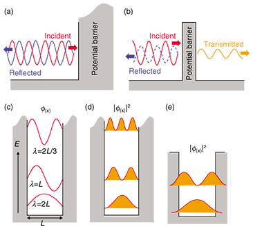
1. IntroductionPhysical phenomena that occur at the nanometer scale cannot be treated by classical physics. Instead, treatment by quantum mechanics is necessary. In quantum mechanics, matter behaves not only as a particle, but also as a packet of waves. The state of the matter can be represented by a wavefunction. By solving the differential equation of the wavefunction, called the Schrodinger equation, under certain given conditions, we can statistically estimate possible phenomena and obtain their time variations. The squared wavefunction corresponds to the probability of a particle existing. In quantum mechanics, there are three well-known fundamental phenomena [1]. (1) Reflection of particle waves and interference When a particle collides with a potential barrier of infinite energy height, it is scattered elastically (energy is conserved). The incident and reflected particle waves interfere with each other because of their coherency. This results in a standing-wave in the existence probability with half the original wavelength of the particle’s wavefunction (Fig. 1(a)). (2) Tunneling effect If there is a potential barrier with finite width and finite energy height higher than the particle’s energy, the probability of the particle being transmitted through the barrier does not reach zero (Fig. 1(b)). This effect is strongly enhanced for a thin barrier. (3) Quantum confinement When a particle is confined one-dimensionally in an infinite potential well (quantum well) of width L, the motion of the particle is restricted. Only the wavefunctions, called subbands, with wavelength λ=2L/n and energy level E=h–2k2/ 2m are allowed, where integer n is the subband index, k=2π/λ is the wave number, m is the effective mass, and h– is Planck’s constant divided by 2π (Figs. 1(c) and (d)). If the barrier height is finite, these wavefunctions penetrate the barriers surrounding the well (Fig. 1(e)).
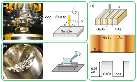
By using semiconductor heterostructures, which are layer structures composed of different semiconductor materials, we can artificially create a potential barrier and quantum well for the electron wavefunction. Semiconductor heterostructure devices, which comprise more complicated layer structures, are extensively used in optical and high-speed electronic devices, supporting our highly networked information society. As semiconductor devices develop and become highly integrated, their quantum mechanical properties, rather than simply the quantity of electrons, will come to dominate their characteristics. Therefore, a method for investigating wavefunctions in real space with nanometer-scale resolution has been desired. For most electrical and optical measurements, however, it is impossible to investigate these characteristics locally. Only statistical averages over large areas can be obtained. The most promising methods are scanning tunneling microscopy (STM) and scanning tunneling spectroscopy (STS) [2], [3], which allow us to observe the spatial distribution of the value corresponding to the squared electron wavefunction at each energy level, called the electron local density of states (LDOS) here, although it is impossible to observe the wavefunction itself. The spatial distribution of the LDOS on semiconductor and metal surfaces has been observed [4], [5]. For semiconductor heterostructure devices, the application of these techniques to cross-sectional surfaces is expected to make possible real-space analyses of the wavefunctions in the devices. However, most attempts, even for a quantum well or a single potential barrier, which are the most fundamental quantum structures, have had limited success so far. Recently, we succeeded in imaging the LDOS on the cross-sectional surfaces of semiconductor heterostructures cleaved in an ultrahigh vacuum (UHV) by low-temperature STS. In this paper, we show spatially and energetically resolved vivid and clear patterns of the LDOS corresponding to the subbands in a quantum well, the electron wave interference at the single potential barrier, and the wavefunction coupling between the quantum wells through the tunneling effect. Our achievements will be invaluable for real-space wavefunction analyses of heterostructure devices. 2. Experimental procedures2.1 STM and STSFirst, the STM system and STS measurement are described briefly (Fig. 2(a)). When conductors become close to each other on the nanometer scale with a bias voltage applied, a tunneling current flows between them across the insulating spatial gap. For STM, the probe tip is attached to a three-dimensional piezoelectric actuator. Bias voltage V is applied to the sample from the grounded tip. The distance Δz between the STM tip and sample is feedback-controlled under a constant tunneling current I. If the tip is scanned parallel to the sample surface (the x-y plane), Δz can be monitored as functions of the x and y positions. As a result, a topographic image of the surface can be obtained with picometer-order resolution in the x, y, and z directions [2]. For STS, using the STM setup, we investigated the tunneling current characteristics by sweeping V. It is known that the normalized differential tunneling conductance [(dI/dV)/(I/V)] (function of V) is proportional to the LDOS [3], which describes the number of states at each energy level that are available for occupation by electrons. The voltage V [V] corresponds to the energy V [eV] from the Fermi level, which is the highest energy level that electrons occupy at low temperature (1 eV ≈ 1.602 × 10⁻¹⁹ J). The energetically integrated LDOS from the bottom of the conduction band (the energy range of available states over the band gap) to the Fermi level becomes the electron density, and the spatially integrated LDOS becomes the density of states (DOS) generally used in condensed matter physics. By scanning the tip, we can image the spatial distribution of the LDOS as a function of the energy. For the experiment, to prevent contamination of the sample surface by impurity absorption and to avoid degradation of the energy resolution by thermal broadening, we used a UHV low-temperature STM. The pressure was less than 10-8 Pa and the temperature was about 5 K (1 K ≈ 8.617 × 10⁻⁵ eV). 2.2 Samples and cleavageThe samples were indium-arsenide/gallium-antimonide (InAs/GaSb) heterostructures, which have been used for mid-infrared optical devices and high-frequency transistors [6], [7]. They were grown by molecular beam epitaxy with a resolution of one atomic layer. To obtain a clean flat surface without impurities, each sample was cleaved in UHV and transferred to the STM without breaking the UHV (Fig. 2(b)). In this way, we succeeded in obtaining a wide flat cleaved surface of more than 10 µm × 10 µm without any atomic steps. A typical STM topographic image of a cleaved sample surface is shown in Fig. 2(c). A clear atom-resolved image was obtained.
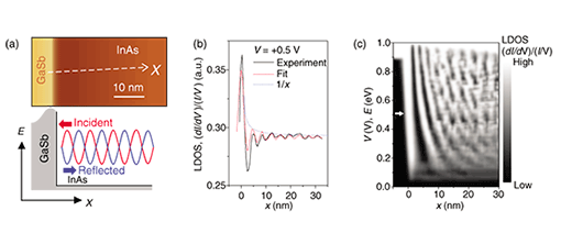
3. Results and discussion3.1 Electron wave reflection and interference at a single potential barrierIn the InAs/GaSb system, the GaSb layer becomes a potential barrier of 0.96 eV from the bottom of the InAs conduction band in the InAs layer (Fig. 2(c)). An STM topographic image of the area around a thick-InAs/GaSb interface on the cleaved sample is shown in Fig. 3(a). Bright regions show the GaSb layer and dark regions show the InAs layer. The contrast difference comes from the difference in tunneling conductance for the layers, not from their real heights. STS measurements were performed by scanning the tip along the dotted arrow normal to the interface. The measured LDOS [(dI/dV)/(I/V)] at V = +0.5 V as a function of the distance from the interface in the InAs layer is shown in Fig. 3(b). There is a clear standing wave of the LDOS, which we attributed to interference between the electron wave incident to the GaSb barrier and the electron wave reflected from the barrier. The curve can be fitted by The LDOS is plotted as functions of the position and energy in Fig. 3(c). The bright region shows a high LDOS. The cross-section at the arrow corresponds to the solid line in Fig. 3(b). As the energy increased, the wavelength of the standing waves became shorter, corresponding to a shorter electron wavelength. From this experiment, we were able to obtain the dispersion relations (energy as a function of wave number) and the effective mass in a nanometer-scale area, both of which are extremely important for applications of semiconductor materials to devices [8].
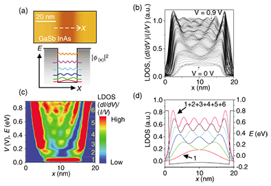
3.2 Quantum confinement in a quantum wellBy growing a thin InAs layer sandwiched between GaSb barrier layers, one can form a quantum well in the conduction band. A typical topographic image of a quantum well on a cleaved surface is shown in Fig. 4(a). The measured thickness of the well was 17 nm. STS measurements were performed on this surface along the arrow. The measured spatial distribution of the LDOS is plotted for each value of V in Fig. 4(b). With increasing V, the number of oscillation peaks increased discretely, indicating subband formation. A color plot of the same data is shown in Fig. 4(c). Here, the oscillation minima in Fig. 4(b) were set to zero for easy visualization. We calculated the LDOS distribution. For STS in the quantum well, the observable LDOS should be the total LDOS for all existent subbands below the energy at V because of the motion parallel to the layers. The calculated results are shown in Fig. 4(d), where the notation ‘1+2+3’ indicates the total LDOS for ground ‘1’, second ‘2’, and third ‘3’ subbands, and so on. The experimental results in Fig. 4(d) agree well with the calculation [9].
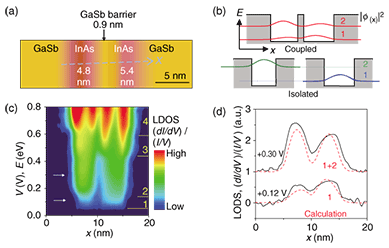
3.3 Coupled double quantum wellAs a demonstration of STS on cleaved heterostructures applicable to more complicated heterostructures, we investigated the LDOS in a double quantum well. An STM topographic image of the sample is shown in Fig. 5(a). A thin GaSb barrier of 0.9 nm was inserted between the InAs wells. The well widths, 4.8 and 5.4 nm, were slightly different from each other. If the quantum wells had been isolated (Fig. 5(b) lower), the LDOS for the ground subband should have been distributed only in the wider quantum well because of the smaller confinement. In other words, the wavefunction should have been completely confined in a single well. When the barrier between the wells was thin enough for tunneling, the wavefunctions between wells were coupled and spread over both wells as a result of the tunneling effect. Therefore, for the ground subband, the distribution of the LDOS could be observed even in the thinner well (Fig. 5(b) upper). The spatial distribution of the LDOS is plotted in Fig. 5(c) as functions of V and the position along the arrow in Fig. 5(a). Clear subband formation was observed. Figure 5(d) shows the spatial distribution of the LDOS for the ground and second subbands corresponding to the cross-sections at the arrows in Fig. 5(c). For the ground subband, the LDOS was distributed not only in the right wider quantum well but also in the left thinner one. This clearly shows the wavefunction coupling and agrees well with the calculation (Fig. 5(d)) [9].
4. ConclusionUsing scanning tunneling spectroscopy on cleaved semiconductor heterostructure surfaces, we succeeded in imaging electron wave interference, quantum confinement, and wavefunction coupling through the tunneling effect, which are fundamental quantum mechanical phenomena. This method is promising for real-space analyses of wavefunctions in devices, which will lead to improved device performance and higher device yields. In addition, we are hopeful that new quantum devices will be developed after unknown physics in nanometer-scale areas have been discovered and clarified. AcknowledgmentsWe thank S. Perraud of LPN-CNRS, France, and Y. Hirayama of Tohoku University for fruitful discussions and C. Janer of ESPCI, France, for help with the experiments. We also thank M. Ueki of NEL-Techno for growing the samples. References
|
||||||||||||||||||||||||