 |
|||||||||||||||||||||||
|
|
|||||||||||||||||||||||
       |
Letters Vol. 6, No. 9, pp. 31–36, Sept. 2008. https://doi.org/10.53829/ntr200809le1 Receiver Frontend IC Technology for Polarization Mode Dispersion Compensation
|
||||||||||||||||||||||

| † | NTT Photonics Laboratories Atsugi-shi, 243-0198 Japan |
|---|
1. Background
With the recent popularization of broadband service via optical fiber access, more transmission capacity is required in the optical core networks. One of the most promising transmission formats for meeting this requirement is differential quadrature phase shift keying (DQPSK) because it offers a high optical signal-to-noise ratio (OSNR) tolerance, dispersion and filtering tolerance, and high spectral efficiency. Recently, wavelength division multiplexing (WDM) systems with 43-Gbit/s DQPSK have started to be deployed in optical core networks in Japan.
For the receiver frontend of the 43-Gbit/s DQPSK transmission system, we have already developed a transimpedance amplifier/limiting amplifier (TIA/LIM) integrated circuit (IC) using indium phosphide (InP) hetero-junction bipolar transistors (HBTs) and a balanced photoreceiver module, which have excellent bit error rate (BER) characteristics [1].
In high-data-rate optical transmission, such as 43 Gbit/s, one of the most important factors limiting the transmission distance is polarization mode dispersion (PMD). This is a phenomenon where the propagation speed of light changes depending on the light's polarization because of the asymmetry in the core of optical fiber. The way PMD affects the received electrical signals is shown in Fig. 1. An optical signal launched into the fiber has two polarization components (depicted in blue and pink), which have different propagation speeds. The blue component reaches the end of the fiber after the pink one. As a result, the received signal is distorted, which degrades the eye-opening.
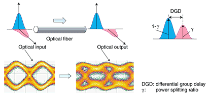
Fig. 1. Effect of PMD on received electrical signal.
To tackle the limitation caused by PMD, we developed an electrical dispersion compensation (EDC) IC for 43-Gbit/s DQPSK. We also developed a trans-impedance amplifier with automatic gain control (TIA/AGC) IC for use with the EDC IC. These ICs, when used in the receiver frontend of a 43-Gbit/s DQPSK transmission system, suppress waveform distortion and improve the BER and thereby extend the transmission distance.
2. Electrical dispersion compensation (EDC)
The features of various dispersion compensation techniques, which include both optical and electrical methods are summarized in Table 1. Optical dispersion compensation (ODC) features a large PMD tolerance enhancement, but the module is large and expensive. EDC is a technology for compensating for the effect of dispersion after optical-to-electrical (O/E) conversion. Its implementations are generally smaller and less expensive than those of ODC. Depending on its signal processing methods, EDC can be classified into digital EDC and analog EDC [2].
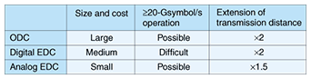
Table 1. Comparison of various dispersion compensation methods.
A typical digital EDC is based on maximum likelihood sequence estimation (MLSE). MLSE-EDC is performed with an analog-to-digital (A/D) converter and digital signal processor (DSP), which are used to infer the original bit sequence. It provides a large improvement in PMD tolerance. However, the clock speed of the A/D converter should generally be not less than double the symbol rate. Because of the limitation in the resolution of A/D converters and the processing speed of DSPs, the applicable symbol rate of MLSE-EDC is currently limited to a maximum of 1010 symbols per second (10 Gsymbol/s).
On the other hand, analog EDC uses analog signal processing. Although the PMD tolerance extension provided by analog EDC, such as a feed-forward equalizer (FFE), is not as large as that of digital EDC, analog EDC is applicable to symbol rates of over 20 Gsymbol/s. It also has the advantage of a small module size and low power. Considering these advantages, we developed an analog FFE EDC IC for 43-Gbit/s DQPSK.
3. Functions of TIA/AGC and EDC ICs in receiver frontend
A block diagram of the DQPSK optical receiver frontend with EDC is shown in Fig. 2. The optical DQPSK demodulator converts a 43-Gbit/s optical quaternary phase-shifted signal into two channels of 21.5-Gbit/s optical intensity-modulated signals. Each channel has a pair of balanced optical signals; these are input into a dual-photodiode (dual-PD).
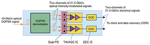
Fig. 2. Block diagram of DQPSK optical receiver frontend with EDC.
The TIA/AGC ICs linearly amplify the input electrical signals and then the EDC ICs compensate for PMD. Here, linear operation of the TIA/AGC is indispensable for the receiver. If the amplifier provides a limiting operation as in the TIA/LIM amplifier, EDC should compensate for the waveform distortion caused not only by PMD but also by the non-linearity of the amplifier, which results in degradation of the PMD tolerance.
4. TIA/AGC IC
To fabricate the ICs, we used InP HBTs. Our InP HBTs have a cutoff frequency of 170 GHz and have already proved to be highly reliable [3]. A block diagram of the TIA/AGC IC is shown in Fig. 3. The IC consists of a TIA core, an AGC amplifier, an output buffer, and a peak power monitor circuit. In the AGC amplifier, the gain of the gain control amplifier is controlled so as to operate as a linear amplifier by the feedback from the amplitude monitor. Therefore, the AGC amplifier outputs a constant voltage swing without saturation. We designed the IC to ensure a constant output voltage amplitude within the optical dynamic range of 6 dB. The peak power monitor circuit is integrated to control the phase difference in the optical demodulator. The circuit detects the received peak signal amplitude and outputs it through the PMON (peak power monitor) terminal.
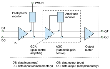
Fig. 3. Block diagram of TIA/AGC IC.
A photograph of the fabricated IC chip is shown in Fig. 4. A fully differential configuration was used for connection with the dual-PD and to stabilize performance against device fluctuation. The chip size is 2×2 mm2 and the power consumption is 0.6 W. The 3-dB bandwidth is 19 GHz and the differential gain is as high as 34 dB. The group delay deviation is only ±10 ps. A balanced photoreceiver module was fabricated by using the TIA/AGC IC and a dual-PD, which integrates two maximized induced current photodiodes (MIC-PDs) [4] and provides a high 3-dB bandwidth of 25 GHz and high responsivity of about 1 A/W.
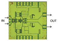
Fig. 4. Photograph of TIA/AGC IC chip.
Output waveforms of the photoreceiver are shown in Fig. 5. The output amplitudes and output waveforms stayed nearly constant in the input optical power range from -9 to -3 dBm, which means that the AGC circuit operated properly. In back-to-back BER experiments, this photoreceiver itself exhibited excellent BER characteristics. We confirmed a Q-value of more than 14.5 dB at OSNR = 19 dB for the PD input power range of 6 dB.
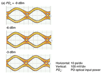
Fig. 5. Output waveforms of TIA/AGC optical receiver.
5. EDC IC
We designed an FFE with a three-tap transversal filter structure (Fig. 6). The FFE IC is composed of an input buffer, two delay circuits, three mixers, two adders, and an output buffer. For linear signal processing, the gain of each component, except for that of the output buffer, is set to nearly unity. In this case, the bit spacing of 45 ps at a bit rate of 21.5 Gbit/s is the designed tap delay for one delay circuit. The delay circuit can be achieved by the transmission lines, but they generally need a large IC area or external components. We therefore used differential delay buffers. In the fabricated IC, even the longest path has a bandwidth of more than 20 GHz. The measured tap delay values differed from the design value by at most 10%.
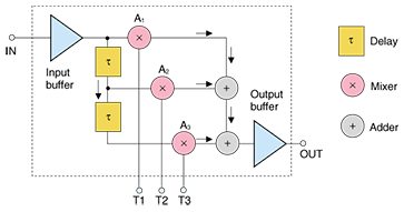
Fig. 6. Block diagram of three-tap FFE EDC IC.
A photograph of the EDC IC chip is shown in Fig. 7. The chip size is 2×3 mm2 and the power consumption is 1.3 W. We examined the performance of the EDC IC by evaluating improvements in electrical waveforms when a differential group delay of 30 ps was imposed by a PMD emulator.
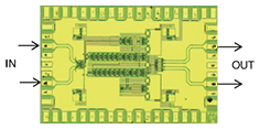
Fig. 7. Photograph of EDC IC chip.
The output waveform of the photoreceiver is shown in Fig. 8(a). Because of the large dispersion, the output waveform is greatly distorted and the eye-opening is very small, which implies poor BER performance. The output waveform of the EDC module connected after the photoreceiver is shown in Fig. 8(b). The widely open eyes indicate greatly improved BER performance. When this EDC module with a fixed tap configuration is used, the transmission distance is expected to be extended by up to 1.5 times [5].
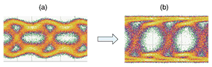
Fig. 8. Output waveforms of (a) optical receiver and (b) EDC module with differential group delay of 30 ps.
6. Future prospects
We will try to reduce the module size by integrating the two 21.5-Gbit/s channels of TIA/AGC ICs into one IC. We also intend to expand the application area of the EDC by using adaptive equalization.
References
| [1] | T. Furuta, K. Yoshino, H. Fukuyama, T. Itoh, and E. Yoshida, “Balanced-photodiode Module Technology,” NTT Technical Journal, Vol. 19, No. 11, pp. 58–61, 2007 (in Japanese). |
|---|---|
| [2] | H. Bülow, F. Buchali, and A. Klekamp, “Electronic Dispersion Compensation,” Proc. of OFC/NFOEC 2007, Anaheim, CA, Mar., 2007, Tutorial, OMG5. |
| [3] | Y. Fukai, K. Kurishima, M. Ida, S. Yamahata, and T. Enoki, “Highly reliable InP-based HBTs with a ledge structure operating at current density of 2mA/µm2,” Proc. of the 17th Indium Phosphide and Related Materials Conference (IPRM 2005), pp. 339–342, Glasgow, UK, 2005. |
| [4] | Y. Muramoto and T. Ishibashi, “InP/InGaAs pin photodiode structure maximising bandwidth and efficiency,” Electron. Lett., Vol. 39, No. 24, pp. 1749–1750, 2003. |
| [5] | E. Yoshida, H. Kawakami, E. Yamada, K. Kubota, Y. Miyagawa, Y. Miyamoto, T. Furuta, T. Itoh, K. Sano, and K. Murata, “Enlargement of PMD tolerance in 43 Gbit/s RZ-DQPSK signal using electrical dispersion compensation without adaptive control,” Proc. of ECOC 2007 3.1.3, Berlin, Germany, 2007. |
 |
|
|---|---|
 |
|
 |
|
 |
|
 |
|