|
|||||||||||||||||||||||||||||
|
|
|||||||||||||||||||||||||||||
       |
Special Feature: Light Source Technologies for Sensing Applications Vol. 7, No. 1, pp. 9–15, Jan. 2009. https://doi.org/10.53829/ntr200901sf2 InAs Quantum-well Distributed Feedback Lasers Emitting at 2.3 µm for Gas Sensing ApplicationsAbstractWe have succeeded in fabricating strained-layer InAs quantum-well active regions on InP with an emission wavelength longer than 2.3 µm by optimizing the growth temperature in metalorganic vapor phase epitaxy. Fabricated distributed feedback lasers exhibit single-mode continuous-wave operation in the temperature range from 15 to 95°C, an emission wavelength exceeding 2.3 µm, and optical output power higher than 20 mW at 25°C. These characteristics are sufficient for practical light sources for mid-infrared-laser-based spectroscopy for sensing environmental gases. 
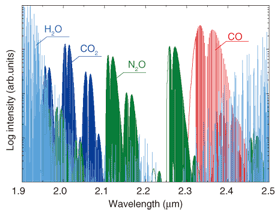
1. IntroductionMid-infrared lasers with an emission wavelength of around 2 µm are very useful for sensing trace gases in environmental monitoring. This is because the strong absorption lines of various gases such as CO2, N2O, and CO are located in this wavelength range and the absorption of water is very low, as shown in Fig. 1. Laser absorption spectroscopy enables us to make measurement systems that provide both a quick response and remote sensing. Tunable light sources with single-mode operation and continuous-wave (CW) output power of several milliwatts are favorable for most sensor applications. Semiconductor lasers fabricated from InP-based materials are attractive candidates because their growth and processing technologies, which have matured through the development of telecommunications lasers, can also be used to fabricate light sources for sensors.
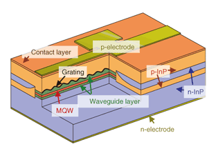
The structure of a conventional InP-based distributed feedback (DFB) laser is shown schematically in Fig. 2. The structural characteristics are as follows. First-order gratings are formed on the upper InGaAsP waveguide layer, and then a p-InP cladding layer is regrown on the gratings. The active region, which is composed of multiple quantum wells (MQWs), is processed into mesa stripes, and these stripes are then buried with p- and n-InP current blocking layers. The grating fabrication and the regrowth process require advanced techniques, which are well established for InP-based lasers. The emission wavelength of a conventional InP-based DFB laser ranges from 1.3 to 1.55 µm. It is difficult to fabricate an InP-based DFB laser emitting at a wavelength longer than 2 µm because the bandgap wavelength of InP-based material is shorter than 1.7 µm when the layer is lattice-matched to an InP substrate.
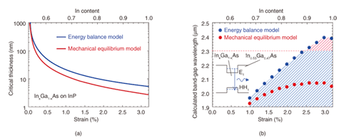
NTT Photonics Laboratories has developed technology for growing high-quality strained-layer InGaAs quantum wells that enables us to fabricate mid-infrared lasers with an emission wavelength longer than 2 µm [1], [2]. In this article, we report our recent results for 2.3-µm wavelength lasers with 3.2%-strained InAs MQW active regions. Section 2 describes an InGaAs MQW on an InP substrate designed to obtain an emission wavelength longer than 2.3 µm. The description includes the In composition and thickness of the quantum well. Section 3 covers certain issues related to the epitaxial growth of strained InAs MQWs. Section 4 reports the device characteristics of the DFB lasers. Section 5 concludes with a brief summary. 2. Design of InGaAs quantum well for wavelengths exceeding 2.3 µmFor InP-based quantum-well structures, the use of an InGaAs layer with a high In content as a quantum well is an effective way to extend the emission wavelength. However, InGaAs quantum wells with an In content higher than 0.53 exhibit compressive strain because they have a larger lattice constant than InP. Therefore, as the compressive strain increases with increasing In content, it becomes difficult to grow a strained InGaAs quantum well without generating defects. The calculated critical thickness, which is defined as the maximum thickness that can be grown without generating any kinds of defects, as a function of the strain (and In content) of an InGaAs layer on an InP substrate is shown in Fig. 3(a). The critical thickness was calculated using two different theoretical models: the mechanical equilibrium model [3] and the energy balance model [4]. For both models, the critical thickness decreases with increasing strain. Although the critical thickness is larger than 10 nm when the strain is less than 1.0%, it decreases to less than 10 nm when the strain is greater than 2.0%. The experimental critical thickness tends to fall between the values calculated with these two models [5]. Thus, the maximum critical thickness obtained empirically is probably the value calculated with the energy balance model. To clarify the emission wavelength that can theoretically be obtained, we calculated the bandgap wavelength of InGaAs quantum wells with the critical thickness shown in Fig. 3(a). The relationship between the calculated bandgap wavelength and the strain for InGaAs quantum wells sandwiched between In0.53Ga0.47 as barriers lattice-matched to InP is shown in Fig. 3(b). Here, the bandgap energy is the energy of the interband transition from an n=1 electron (E1) state to an n=1 heavy hole (HH1) state. The bandgap wavelength for the energy balance model is longer than that for the mechanical equilibrium model because the quantum energy level becomes lower as the well thickness increases. The bandgap wavelength becomes longer owing to the large contribution made by the reduction in the bandgap energy of a quantum well with increasing In content while the critical thickness decreases. This indicates that an increase in In content of an InGaAs quantum well is more effective at extending the emission wavelength than an increase in the well thickness. From the calculation shown in Fig. 3(b), we can estimate the required strain to be greater than 2.5%, which corresponds to an In content of greater than 0.90, if we are to obtain an emission wavelength longer than 2.3 µm. On the basis of these calculations, we investigated the fabrication of an InAs quantum-well structure with a strain of 3.2% to achieve an emission wavelength longer than 2.3 µm.
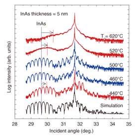
3. Fabrication of InAs quantum wellAlthough an emission wavelength longer than 2.3 µm can theoretically be obtained by using an InAs quantum well, it is difficult in practice to grow an InAs quantum well on an InP substrate because of the large lattice mismatch between InAs and InP, which can be as much as 3.2%. In general, a reduction in growth temperature is effective for strained layer growth because it reduces the surface diffusion length of adatoms [6] and increases the critical layer thickness [7]. Therefore, we attempted to grow InAs/In0.53Ga0.47As MQW structures on InP substrates by reducing the growth temperature. All the samples were grown by metalorganic vapor phase epitaxy (MOVPE). We used growth temperatures in the range from 440 to 620°C to investigate the influence of temperature on the InAs/InGaAs MQW structures. X-ray diffraction (XRD) spectra of InAs MQWs grown at different temperatures along with a simulated spectrum obtained using the dynamical theory [8] are shown in Fig. 4. The InAs quantum wells of all the samples were 5 nm thick. No satellite peaks can be seen in the spectra of the samples grown at 520 and 620°C, and the peaks of the envelope curves, which correspond to the lattice constants of the well layers along the growth direction, are shifted to a higher angle than in the simulation. For the samples grown at 460 and 500°C, the spectra have clearly defined satellite peaks and agree well with the simulation spectra. With growth at 440°C, the peaks of the envelope curves are again shifted to a higher angle, although satellite peaks can be seen. We interpret these results as follows. Due to the large strain, three-dimensional growth occurred easily on the growing surface of the InAs layer. The strain relaxation caused by the three-dimensional growth was enhanced at higher growth temperatures because the surface diffusion length of adatoms on the growing surface increased as the growth temperature increased [6]. The peak shifts of the envelope curves and the absence of satellite peaks in the spectra of the samples grown at 520 and 620°C indicate that strain relaxation occurred in the InAs wells. Reducing the growth temperature to the 460–500°C range suppressed the strain relaxation and yielded flat interfaces between the wells and the barriers. However, when the growth temperature was reduced to 440°C, we could not obtain an InAs MQW of the desired quality because of Ga incorporation in the InAs well layers. The XRD results reveal that InAs/InGaAs MQWs with good structural characteristics could be obtained only in a narrow MOVPE growth temperature range of 460 to 500°C.
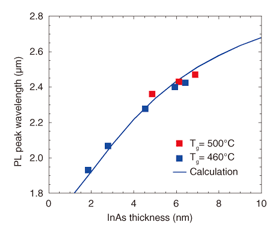
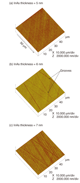
On the basis of the above results and interpretation, we next attempted to control the emission wavelength of the MQW by controlling the thickness of the InAs quantum well. The dependence of the photoluminescence (PL) peak wavelength of the MQWs grown at 460 and 500°C and the calculated bandgap wavelength on the thickness of the InAs wells [8] are shown in Fig. 5. The PL peak wavelength increased from 1.93 to 2.47 µm as the InAs thickness increased from 2 to 7 nm. We achieved PL peak wavelengths longer than 2.3 µm for MQWs with an InAs thickness greater than 5 nm. In addition, these experimental values agree well with the calculated results. It is evident that the bandgap wavelength was well controlled over a wide wavelength range by adjusting the thickness of the InAs quantum well. Although we could extend the PL wavelength beyond 2.3 µm by using the InAs quantum well, the surface morphology deteriorated with increasing well thickness. Atomic force microscope (AFM) images of the surfaces of InAs MQWs with different well thicknesses grown at 500°C [8] are shown in Fig. 6. A featureless surface was obtained for an InAs thickness of 5 nm, as shown in Fig. 6(a). However, there were many grooves on the surface of the MQWs with InAs thicknesses of 6 and 7 nm, as shown in Figs. 6(b) and (c), respectively. The number of grooves increased as the InAs thickness increased. These grooves may be attributed to defects generated by the strain relaxation of the InAs quantum well because the InAs thickness exceeded the critical layer thickness estimated using the energy balance model shown in Fig. 3(a). On the basis of the above results, we chose to use an InAs/InGaAs MQW structure with a well thickness of 5 nm as the active region of a laser emitting at 2.3 µm.
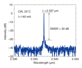
4. Device fabrication and characteristicsThe fundamental processes for fabricating 2-µm wavelength DFB lasers are well established, as mentioned in Section 1. We fabricated our DFB lasers as follows. First, an active region composed of a separate-confinement-heterostructure MQW was grown at 500°C by MOVPE. The MQW active region consisted of four 5-nm-thick InAs wells and five 20-nm-thick In0.53Ga0.47As barriers. The lower separate confinement heterostructure (SCH) layer was a 100-nm-thick InGaAsP layer with a bandgap wavelength of 1.3 µm and the upper SCH layers were 100-nm-thick InGaAsP layers with bandgap wavelengths of 1.3 and 1.1 µm. Next, first-order corrugations were formed on the upper SCH layer with a bandgap wavelength of 1.1 µm by using electron beam lithography and wet etching. Then, a p-InP cladding layer was grown on the corrugated surface. A 2.0-µm-wide mesa stripe was formed on the wafer and p-n-blocking layers were then grown around the stripe using mesa-defining SiO2 as a regrowth mask. Finally, a p-InP cladding layer and p+-InGaAsP contact layers were grown. All regrowth was carried out using MOVPE at a growth temperature of 600°C. After contact metallization, the wafer was cleaved into bars with a 900-µm-long cavity. The facets of the DFB-laser bars were coated with anti-reflection and high-reflection films [9]. The emission spectrum during CW operation of the DFB laser with a Bragg wavelength of 2.330 µm is shown in Fig. 7. The emission wavelength of the DFB mode was 2.337 µm, which agrees well with the designed Bragg wavelength. This is the longest reported emission wavelength for InP-based DFB lasers using the interband transitions between the conduction and valence bands. The submode suppression ratio was higher than 30 dB, which is sufficient for light sources for sensor applications.
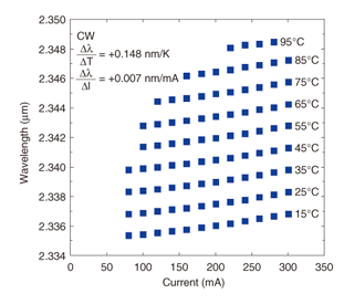
For practical use in trace-gas sensing applications, the emission wavelength of the light source must be tunable over a range of several nanometers. The relationship between the emission wavelength of the DFB laser and the injection current with heatsink temperature as a parameter is shown in Fig. 8. The emission wavelength of the DFB laser changed from 2.335 to 2.348 µm as the heatsink temperature increased from 15 to 95°C. The wavelength shift with increasing temperature was fairly constant at 0.148 nm/K, which is about the same as that of the 1.55-µm-wavelength DFB laser. This indicates that the emission wavelength of the DFB laser is mainly determined by the refractive index, which means it can be well controlled by the periodicity of the grating in the same way as that of a 1.55-µm-wavelength DFB laser. On the other hand, the current-tuning rate of the wavelength was almost constant at 0.007 nm/mA in the temperature range from 15 to 95°C. Such a constant tuning rate enables the emission wavelength to be finely controlled.
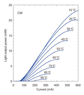
Applications that use laser spectroscopy require not only single-mode operation but also high output power. The CW light output power of the DFB laser versus injected current at heatsink temperatures of 15 to 95°C is shown in Fig. 9. The threshold current and the slope efficiency at 25°C were 61 mA and 0.054 W/A, respectively. The maximum output power was as high as 20 mW at 25°C and was 4 mW even at 75°C. Such an output power is suitable for light sources in spectroscopic applications [10].
5. ConclusionWe demonstrated high-performance DFB lasers with emission wavelengths longer than 2.3 µm that use InAs MQWs on InP as the active regions. First, we confirmed that an emission wavelength longer than 2.3 µm could theoretically be obtained by using an InAs quantum well within the critical thickness. In fact, we achieved a PL emission longer than 2.3 µm for a 5-nm-thick InAs MQW without any structural degradation by reducing the MOVPE growth temperature to between 460 and 500°C. The DFB lasers fabricated using the InAs MQW as an active region exhibited CW single-mode operation at heatsink temperatures of 15 to 95°C. An emission wavelength longer than 2.3 µm was obtained, and the wavelength could be easily tuned by altering the injection current and the heatsink temperature. The output power was higher than 20 mW at 25°C, which is sufficient for practical light sources for gas sensing. References
|
||||||||||||||||||||||||||||