|
|||||||||||||||||||||
|
|
|||||||||||||||||||||
       |
Special Feature: Applied Technology for Millimeter and Terahertz Electromagnetic Waves Vol. 7, No. 3, pp. 23–28, Mar. 2009. https://doi.org/10.53829/ntr200903sf4 Inspection of Concrete Structures Using Millimeter-wave Imaging TechnologyAbstractIn this article, we introduce a new imaging device developed by NTT that uses millimeter-waves to detect surface cracks in concrete. It should lead to inspection technologies for assessing the durability of concrete structures—something that is urgently needed because of concern about structural deterioration with age and faked earthquake-proof certification. 
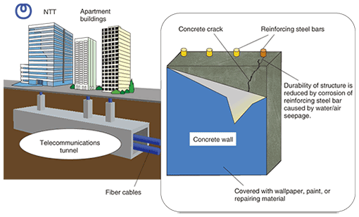
1. Millimeter-wave imaging technologyMillimeter waves are electromagnetic waves with wavelengths in the millimeter range (corresponding to a frequency range from 30 to 300 GHz). Since they can penetrate materials like clothes, plastics, and mist, research and development of millimeter-wave imaging has become highly active in recent years. However, the spatial resolution of quasi-optics millimeter-wave imaging is limited to a few millimeters by their wavelength; therefore, applications have been focused mainly on security use such as airport security gates and aviation monitoring systems that detect objects several centimeters in size [1]. On the other hand, NTT Laboratories has investigated millimeter-wave imaging for detecting objects in the submillimeter range by utilizing the features of near-field imaging [2]. In this article, we introduce our latest results and explain how we overcame the difficulties in achieving the high resolution and high-speed imaging needed to implement a practical device. 2. Importance of inspecting concreteIn order to provide its communication services, NTT has built a lot of concrete structures such as telecommunications buildings and tunnels across the whole of Japan. Some of those built during Japan’s period of rapid growth are beginning to deteriorate due to aging. NTT has developed inspection technologies to assess their durability and has been proactively managing the maintenance. These inspection technologies developed by NTT also hold great promise for other general concrete structures such as apartment buildings and roadways, so they may be applicable to a recent issue of great concern in Japan, which is faked earthquake-proof certification of apartment buildings that may actually be substandard. 3. Durability assessment through crack inspectionOne of the most important aspects of assessing the durability of concrete structures is surface crack inspection. As shown in Fig. 1, when cracks appear on a concrete surface, water and air can penetrate the concrete and attack the reinforcing steel inside causing the steel to corrode. As a result, the strength of the concrete structure decreases. To prevent this sort of deterioration, it is important to detect and repair these surface cracks as early as possible. Deterioration is usually caused by cracks with a width of 0.4 mm or more, so preventative maintenance should be applied to cracks with a width of 0.2 mm or more [3].
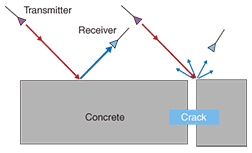
If the concrete surface is exposed, cracks can be detected by visual inspection. However, the walls of buildings and tunnels are often covered with paint, wallpaper, or repairing material, so it is difficult to detect surface cracks by visual inspection. When visual inspection is not possible, ultrasonic waves or x-rays that can pass through the obstructing material are usually used. However, ultrasonic waves are not suitable for finding fine surface cracks of submillimeter width, although they can be used for measuring the depth of cracks that are over 1 mm wide. Using x-rays is also difficult when the far side of the target object is not accessible because the transmitting and receiving sensors must face each other. There are also safety concerns about the use of x-ray equipment, and operators are required to have special qualifications. For these reasons, it has been difficult to use existing technologies to detect surface cracks in unexposed concrete. 4. Approach using millimeter wavesNTT Laboratories investigated the use of millimeter waves as an imaging medium to develop technology for detecting concrete surface cracks. Although millimeter waves penetrate wallpaper and wall coverings, they do not penetrate concrete deeply; nevertheless, they are applicable to surface inspections. Millimeter-wave imaging methods can be categorized into two general types: passive imaging, in which millimeter-waves radiated from an object itself are detected, and active imaging, in which the object is illuminated with external millimeter-wave radiation and the reflection or transmission is detected. For example, warm objects like the human body emit black-body radiation including millimeter-band waves, so passive imaging can be applied to detect concealed items under clothes by using the human body as a backlight (a source of millimeter-wave radiation). On the other hand, objects like concrete structures do not emit detectable amounts of millimeter waves, so an active imaging method using external millimeter-wave radiation is required [4]. When millimeter waves are directed at a concrete surface at an angle, reflections from smooth areas propagate in a single direction, while reflections from crack edges scatter randomly in all directions. Thus, if the transmitter and receiver are positioned opposite each other, as shown in Fig. 2, cracks can be detected by measuring the intensity of reflection.
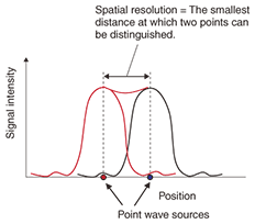
5. Detection of sub-wavelength cracksHere, we explain how cracks can be detected with millimeter-wave imaging in terms of a point wave source. The spatial resolution of a quasi-optics imaging system in the Fraunhofer region is generally on the order of the wavelength. Spatial resolution is defined as the smallest distance at which two points of equal brightness can be distinguished separately. As shown in Fig. 3, the radiation pattern observed from a point wave source does not appear as an infinitely small point, but as a distribution spread out over a width equal to the wavelength. Thus, as the positions of the point wave sources become closer, it becomes more difficult to distinguish the individual points. This is why “it is generally not possible to see objects smaller than the wavelength.”
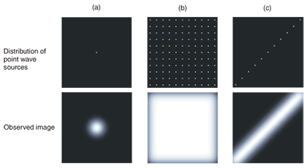
Millimeter waves have wavelengths in the 3–4-mm range, whereas we need to detect cracks about 0.2 mm wide during an inspection. How is it possible to detect cracks with a width of only one-tenth of the wavelength? We utilize the relationship between the distribution of point sources and its image in two-dimensional space. Figure 4(a) shows a single point source in the center of the figure. In Fig. 4(b), many point sources are arranged in a grid; here, it is impossible to know the distribution of point sources because they are close together and appear overlapped in the observed image. This is the effect of it being impossible to see objects smaller than the wavelength, as mentioned above. However, in Fig. 4(c), the point sources are arranged in a line, so we can recognize the rough shape of the line in the observed image, even though individual points cannot be seen separately.
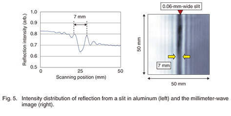
We can take advantage of this visual characteristic to detect fine cracks using millimeter waves. An operator looking at a millimeter-wave image can identify a contour of a crack approximately, even if the image looks somewhat blurred. This is similar to how we can recognize letters or human faces even if a photograph is slightly out of focus. The results of an experiment are shown in Fig. 5. A 0.06-mm-wide slit was created by abutting two plates of aluminum, which has a permittivity similar to that of concrete, and the intensity distribution of the reflection was measured using the millimeter-wave transmitter/receiver. The wavelength of the millimeter-waves used was 4 mm, and the transmitter/receiver was positioned 10 mm from the aluminum plates. In the resulting graph and image, we can recognize the 0.06-mm slit as a blurred 7-mm wide valley in the reflection.
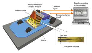
6. Development of Crack ScanWe have developed a nondestructive inspection device, called “Crack Scan”*, which uses the penetrating abilities of millimeter waves and the shape characteristics of the cracks. A key technology for its design is an arrayed detector. Obtaining an image by scanning a single detector in two dimensions would be time-consuming, so we created a one-dimensional array of detectors to enable high-speed scanning (Fig. 6).
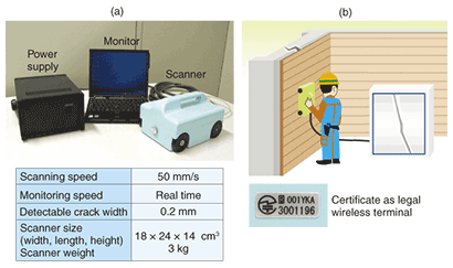
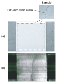
The transmitter uses a Gunn diode and horn antenna directed at the concrete wall surface to emit a millimeter-wave signal. This is amplitude modulated with a square wave having a frequency ranging from several tens to hundreds of kilohertz. The center frequency of the millimeter-wave is 76.5 GHz and the output power is under 10 mW, to conform to the Japanese radio law. The detector uses Schottky-barrier diodes and planar slot antennas to detect the reflection from the concrete surface. The number of detectors is 32, and the aperture of a slot antenna is 1.6 mm. The intensity of the reflection is converted to a voltage by the diode rectifier and digitized with an analog-to-digital converter. The digitized signal is sent to a personal computer and synchronized with the encoder distance signal. Then a two-dimensional image of the concrete surface is plotted on the monitor. The specifications and operating procedure for Crack Scan are shown in Fig. 7. The operator holds the main unit to scan the concrete surface and can identify cracks in real time by observing the image on the monitor. An experimental result is shown in Fig. 8; a 0.35-mm-wide crack covered by a 7-mm thick ceramic tile was detected. This crack scanner can be used through materials such as plastic, rubber, glass, and paint in addition to ceramic.
7. Concluding remarksIn 2008, Airec Engineering Corp., an NTT Group company, began working to commercialize Crack Scan. The device was also exhibited to approximately 400 people related to civil engineering and construction in sessions on nondestructive inspection at five locations (Hokkaido, Saitama, Osaka, Hyogo, and Hiroshima) to further explore needs and clarify technical problems. From these demonstrations to potential users, we received suggestions that the range of applications could be expanded even further if the detection accuracy were improved. Meeting this requirement will probably require the addition of other technologies like image processing to generate a sharper image. We will continue to work on improving the performance of this technology, based on our discovery that fine cracks can be detected by millimeter-wave imaging, in order to explore new application fields besides structural inspection. References
|
||||||||||||||||||||