|
|||||||||||||||||||||||||||||||||
|
|
|||||||||||||||||||||||||||||||||
       |
Letters Vol. 7, No. 12, pp. 44–50, Dec. 2009. https://doi.org/10.53829/ntr200912le2 Channelized Tunable Dispersion Compensator Consisting of Arrayed-Waveguide Grating and Liquid Crystal on SiliconAbstractWe describe a channelized tunable optical dispersion compensator (TODC) consisting of an arrayed-waveguide grating and a liquid-crystal-on-silicon device, which compensates for the chromatic dispersion of wavelength channels independently. We devised a novel double-pass configuration for a channelized TODC with increased bandwidth and demonstrated 40-channel independent compensation. We obtained chromatic dispersion of 400 ps/nm with a 3-dB bandwidth of 52 GHz, which is twice the width obtained with the conventional single-pass configuration. This TODC replaces 40 conventional TODCs with a single module, so it is a promising candidate for use in future networks. 
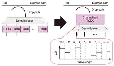
1. IntroductionA tunable optical dispersion compensator (TODC) is an indispensable device for a reconfigurable optical add/drop multiplexed (ROADM) network with a high transmission bitrate such as 40 Gbit/s or higher. In such ROADM networks, the transmission length and chromatic dispersion (CD) vary when a routing path is switched at the ROADM node. The TODC offers the adjustability needed to handle such CD changes. TODCs have already been reported using a number of technologies including lattice filters, etalons, fiber-Bragg gratings, and spectrometer-based TODCs [1]–[5]. A conventional TODC compensates for an optical signal with a single CD value, so one TODC is required for each wavelength division multiplexing (WDM) channel to obtain a different compensation value for each channel independently. As shown in Fig. 1(a), this approach is costly because it needs a large number of TODCs. A channelized TODC (Fig. 1(b)), which can set different CD values for different WDM channels independently, is attractive for use in such a system because it reduces the device count as well as the power consumption of the network.
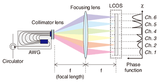
Channelized TODCs with a spectrometer-based configuration consisting of various grating and spatial light modulator (SLM) devices have been demonstrated. In these studies, a microelectromechanical system (MEMS) mirror array [6], [7] or a liquid-crystal-on-silicon (LCOS) device [8] was used as the SLM. However, since a bulk grating was used as the spectrometer, it was difficult to obtain a large CD (~400 ps/nm) because the diffraction order of a bulk grating is small. To obtain a large CD with a spectrometer-based TODC, it is advantageous to use a highly dispersive grating as the spectrometer, such as a virtually imaged phased array or an arrayed-waveguide grating (AWG). The AWG is fabricated using planar lightwave circuit (PLC) technology, which has several advantages including reliability, design flexibility and mass producibility. In this report, we describe a spectrometer-based TODC consisting of an AWG as a spectrometer and an LCOS as the SLM. We have demonstrated six-channel (6-ch) independent CD compensation using a single-pass optical configuration. In addition to this configuration, we also describe a double-pass configuration that enabled us to increase the channel count of the channelized TODC without narrowing its transmission bandwidth and demonstrate 40-channel TODC operation with a 100-GHz channel spacing. 2. Single-pass channelized TODC: principle, design, and characteristicsThe configuration of a channelized TODC consisting of an AWG and an LCOS is shown in Fig. 2. The LCOS is placed on the image plane of a 2-f type focusing system. An optical signal is fed into the AWG via a circulator and is dispersed by the AWG. The signal is then focused onto the LCOS by a focusing lens in the x direction and by a focusing and collimating cylindrical lens in the y direction. The LCOS, which has a large number of fine phase modulator pixels on the dispersion axis (x), modulates the wavefront of the incoming light. The light reflected by the LCOS travels along the incoming light axis, re-enters the AWG, and is output from the AWG to the circulator. We set the phase distribution (hereafter phase function) of the LCOS in a quadratic form Φ(x), as shown in Fig. 2. The CD value D provided by the system is given by 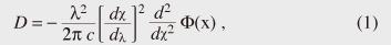 where c, λ, and x are the speed of light in vacuum, the signal wavelength, and the position on the LCOS in the x direction, respectively [9]. The second term dx/dλ represents the dispersion of the AWG spectrometer on the LCOS surface. As derived from the equation, the quadratic coefficient of the phase function Φ(x) determines the CD. There are two ways to obtain a large CD: use a highly dispersive AWG or a large quadratic coefficient. However, since the phase shifts provided by the LCOS are limited to a maximum of 2π, the phase function is folded every 2π, which is analogous to a Fresnel lens.
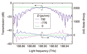
In general, with a spectrometer-based TODC, the transmission spectrum for each channel is Gaussian, and the transmission bandwidth is inversely proportional to the absolute value of the CD. Thus, as the absolute CD value becomes large, the transmission bandwidth decreases. This is understood from the fact that the phase mismatch between the incident and reflected fields at the LCOS becomes significant if the phase function becomes steep. This causes a loss increase near the channel edge where the differential of the quadratic phase function is large. The phase mismatch also becomes large when the beam waist size at the LCOS is large. On the other hand, if the waist size is too small, the effect of the discontinuity of the LCOS pixels cannot be ignored. So we have to optimize the beam waist size of the focusing beam. We built the setup by using an AWG with a free spectral range of 1000 GHz to cover the total bandwidth of six channels with a 100-GHz spacing. The focal length was set at 100 mm. The beam waist diameter was set at eight times the pixel size. The measured single-channel characteristics of the 6-ch TODC are shown in Fig. 3. In this figure, the slope of the group delay (GD) corresponds to the CD. We also obtained similar characteristics for other channels and confirmed independent 6-ch operation. As seen in Fig. 3, we could successfully obtain both positive and negative CDs with absolute values of 800 ps/nm. The 3-dB transmission bandwidth was about 35 GHz with dispersion of ±800 ps/nm, while no degradation was observed when CD was set to 0 ps/nm. The transmission bandwidth was limited by both the Gaussian transmission characteristics and ripples at specific wavelengths around the channel edge. These ripples were caused by interference with an unwanted reflection from the TODC optics. If we can eliminate this interference, the transmission bandwidth should be sufficiently wide for high-bitrate network applications.
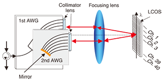
3. Double-pass configuration for high-channel-count TODC3.1 DesignIf we design a channelized TODC to compensate for the CDs of more WDM channels using an LCOS of limited size, then a wider total bandwidth should be assigned to the x-direction length of the LCOS. This means that the linear dispersion dx/dλ in Eq. (1) becomes small and a steeper quadratic phase function must be used to obtain the same CD compensation. Because the steep phase function causes bandwidth narrowing, as described above, this simple approach to raising the channel count is unsuccessful. To avoid the bandwidth narrowing that originates from the slope of the phase function, we devised a new double-pass optical configuration for the channelized TODC (Fig. 4) [10]. It consists of two AWGs, an LCOS, and lenses. Unlike the single-pass TODC shown in Fig. 2, the new setup uses a second AWG to expand the transmission bandwidth. This second AWG is composed of only arrayed-waveguides (i.e., without any slab waveguides) with a reflection mirror at one end. Both AWGs have the same path length difference and waveguide separation, so they have the same angular dispersion. The optical system consists of a folded double-telecentric lens. The setup functions in the following way.
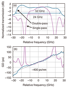
An optical signal fed into the first AWG is dispersed and focused onto the surface of the LCOS through focusing and collimating cylindrical lenses. Then, the LCOS gives the signal a wavelength-dependent phase shift with a quadratic form. The optical signal is then reflected to the focusing lens. Here, the angle of reflection depends on the slope of the quadratic phase function and varies with wavelength. In other words, an LCOS with a quadratic phase distribution acts as a convex or concave mirror. If we return the reflected signal directly to the first AWG in the conventional way, this angle mismatch between the incident and reflected beams causes a passband decrease. When we introduce the reflected signal at the second AWG and reflect it again with the mirror at the end of the arrayed waveguides, as shown by the red arrows in Fig. 4, the beam traces the same incidence path to the first AWG and is output from it. This is because the two AWGs are designed to be identical and to have the same angular dispersion. In other words, the output angle of the beam from the second AWG is determined solely by wavelength. The wavelength-dependent angle deviation on the LCOS side is converted into beam displacement on the AWG side. Therefore, if the second AWG has an aperture wide enough to avoid vignetting, the signal returns to the first AWG with no loss. As a result, the bandwidth reduction is less severe. In addition, the optical signal passes through the LCOS twice in this configuration. Therefore, the CD value is also doubled. 3.2 TODC characteristicsWe designed and fabricated AWGs with a free spectral range of 6 THz to cover the total bandwidth of 40 channels with a 100-GHz spacing and a center wavelength of 1.59 μm by using a 1.5% index contrast silica-based PLC. The linear dispersion of the AWGs was set so that 64 pixels of the LCOS covered a 100-GHz optical frequency range. The focal length was set to 165 mm. The beam waist diameter on the LCOS was six times the pixel width. We then compared the conventional single-pass and new double-pass configurations by changing the LCOS orientation so that the reflected beam returned directly to the first or second AWG. The measured transmission and GD characteristics when the device was set with a chromatic dispersion of around -400 ps/nm are shown in Fig. 5. The 3-dB bandwidths of the single- and double-pass configurations were 24 and 52 GHz, respectively. As seen in the plots, the transmission bandwidth and the linear region of the GD were widened in the double-pass configuration. In addition, the large GD ripples induced in the single-pass TODC were suppressed in the double-pass configuration. It is known that the ripples appear where the phase function crosses the π level [9]. In the double-pass configuration, the ripples were pushed to the outside of the relative bandwidth because the phase function of the double-pass TODC can have a gentler slope to obtain the same CD value.
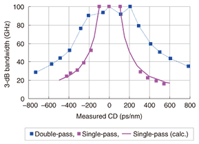
The relationship between the dispersion setting and the 3-dB transmission bandwidth is summarized in Fig. 6. With the single-pass TODC, as expected, the relationship followed the theoretical limitation, namely the bandwidth was inversely proportional to the CD. On the other hand, the bandwidth of the double-pass TODC was wider than that of the conventional one. However, we observed a slight degradation in the bandwidth, which should have remained constant regardless of the CD setting. We think that this bandwidth degradation was induced by some misalignment of the optics such as torsion of the cylindrical lenses that were glued to the PLCs. This misalignment could have prevented the steered beam from coupling efficiently with the second AWG. From a practical viewpoint, the double-pass TODC was able to achieve a CD value of ±400 ps/nm with a 50-GHz bandwidth, which is wide enough for a transmission bitrate of 40 Gbit/s. The insertion losses were 8.8 and 15.2 dB for the single- and double-pass configurations, respectively. By improving the alignment of the optics, we should be able to widen the passband and reduce the insertion loss.
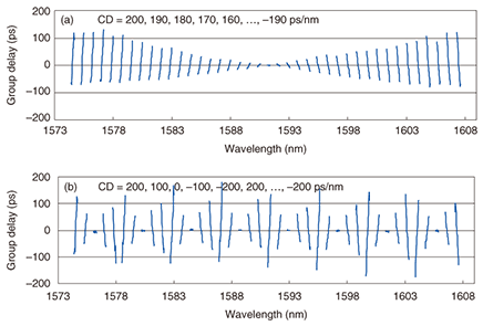
Typical GD spectra for the channel-by-channel operation of the 40-wavelength channelized TODC with the double-pass configuration are shown in Fig. 7. The 40 successive channels with a 100-GHz spacing were simultaneously and independently provided with CD values of (a) 200, 190, …, -190 ps/nm and (b) -190, -180, …, 200 ps/nm. The 40-GHz frequency ranges for the channels were reflected in the plots. As seen in Fig. 7, we successfully achieved channel-by-channel operation for 40 different WDM channels.
4. ConclusionWe demonstrated channel-by-channel CD compensation by using a spectrometer-based channelized TODC comprising an AWG and an LCOS, which is capable of controlling the CDs of WDM channels independently. A maximum CD of ±800 ps/nm with a 3-dB bandwidth of 35 GHz was obtained using the conventional single-pass optical configuration. With our novel double-pass configuration for a channelized TODC with a higher channel count, we demonstrated 40-wavelength channel-by-channel TODC operation. We obtained a CD of 400 ps/nm with a 3-dB bandwidth of 52 GHz, which is twice that obtained with the single-pass configuration. This channelized TODC replaces 40 conventional TODCs with a single module, so it is promising for use in future networks. References
|
||||||||||||||||||||||||||||||||