|
|||||||||||||||||||||||
|
|
|||||||||||||||||||||||
       |
Special Feature: KTN Crystal Technologies Vol. 7, No. 12, pp. 21–26, Dec. 2009. https://doi.org/10.53829/ntr200912sf4 High-resolution KTN Optical Beam ScannerAbstractKTa1-xNbxO3 (KTN) enables us to construct compact, fast optical beam scanners based on a new principle unique to KTN. In this article, we clarify the factors determining the scanning resolution and describe a multipass scheme that is effective for increasing the resolution achievable with the existing degree of crystal homogeneity. The resulting improvements in resolution will make KTN scanners applicable to a broader industrial arena. 
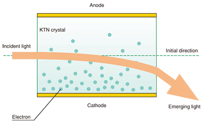
1. IntroductionConsider a KTa1-xNbxO3 (KTN) crystal sandwiched between a pair of electrodes. As light travels though the crystal parallel to the electrodes, we apply a voltage between the electrodes. Voilà! The direction of the light emerging from the crystal varies according to the voltage. This phenomenon was first discovered in 2006 here in NTT Laboratories [1]. The electron deflector, which changes the direction of movement of electrons by applying an electric field, is well known. Using KTN crystal, we made a deflector for light rather than electrons, as shown in Fig. 1. Since then, we have managed to find an explanation for this odd phenomenon: electrons are injected into the crystal through the cathode, forming a space charge distribution that, in turn, modifies the electric field between the electrodes so that the field becomes uneven. Such a field, combined with the electro-optic (EO) effect, which the KTN crystal exhibits, causes the light path to be bent [2]. Here, for the space charge to accumulate under a practicable voltage, we need an exceptionally large value of the electric permittivity ε. Moreover, for the uneven field to produce a linear change in the refractive index, which eventually bends the light path, the EO effect is restricted to being of the second order (i.e., Kerr-type). KTN meets both these requirements simultaneously, and it is almost unique among crystals in manifesting the optical deflector function based on such space-charge-controlled EO effect.
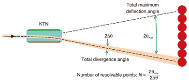
Thus, the KTN optical scanner is a kind of EO device. Accordingly, it is fast and might be able to follow a sub-gigahertz control voltage, as has been demonstrated for KTN modulators [3]. On the other hand, the refractive index gradation is induced all over the crystal and the bending effect accumulates along the entire light path in the crystal, so a fairly large deflection can be obtained. In this regard, the KTN scanner is quite different from previously reported prism-based devices (e.g., [4]), where the bending effect is merely localized at the air-crystal interfaces. Thanks to its combination of these usually contradictory properties, i.e., high speed and large attainable deflection, KTN is expected to have numerous new applications. 2. Resolution of optical scannersIn the KTN scanner, the optical beam should be focused onto the crystal with a small spot diameter of less than the crystal thickness d, so that the beam can pass through the narrow gap between the electrodes. Diffraction causes such a beam to inevitably have a fairly large divergence angle, as shown in Fig. 2. Provided that the change in deflection angle caused by the applied voltage is smaller than the inherent divergence angle Δθ, the deflection angle change is hardly discernible because it is overwhelmed by divergence. From this viewpoint, the total divergence angle 2Δθ is like a granularity of the deflection angle for an optical scanner. Furthermore, the total range of deflection angle 2θmax normalized by the divergence angle, i.e., N = 2θmax/2Δθ, represents how many points can be distinguished, namely, the number of resolvable points.
While we might be able to vary either the deflection angle range or the divergence angle though angular magnification provided by subsequent optics, we cannot vary their ratio N. Therefore, the number of resolvable points serves as the principal performance index of optical scanners. KTN scanner resolution given by N of ~20 has previously been reported [5]. In comparison, the polygon mirrors typically used in laser printers, for example, have no need for beam focusing and boast a resolution of over 1000. The KTN scanner features much faster controllability, and might not necessarily compete in terms of high-end precision. Nevertheless, improved resolution would open up a broader application area for it. 3. Limiting factor for resolutionAn analysis of the space-charge-controlled EO effect gave us the following formula for the maximum deflection angle θmax: 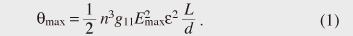 Here, d denotes the distance between the electrodes, i.e., the crystal thickness; n, ε, and g11 respectively express the refractive index, permittivity, and second-order electro-optic coefficient of the KTN crystal; and Emax represents the maximum electric field that can be imposed on the crystal. Since the electric field reaches its maximum value of 1.5 times its average of V/d right in front of the anode when the space charge is formed, it can be translated into a value Vmax = (2/3)Emaxd for the maximum voltage that can be applied to the crystal. On the other hand, for a light beam of wavelength λ, the divergence angle accompanying a radius of beam-waist w is expressed as Δθ = λ/(πw). This, along with Eq. (1), gives the following expression for the number of resolvable points N.  As for the material constants of KTN, the refractive index n is 2.29 [6] at a wavelength λ = 633 nm, while the second-order electro-optic coefficient has been reported to be g11 = 0.136 m4C−2 [7]. The electric field upper-bound Emax is known empirically to be around 600 V/mm. By plugging these values into Eq. (2) and using permittivity of 15,000, we get N = 25.7 (w/d)L, where size factors w, d, and L are all assumed to be expressed in millimeters. The beam diameter 2w cannot exceed the crystal thickness d by nature. Moreover, in our case, for an optical scanner, it is essential to leave room for the deflected beam. A simple geometric consideration tells us that to maximize N, the optimal beam diameter should be half the crystal thickness, namely, w/d = 1/4. Taking this into account, we devised a rule of thumb: N = 6.4 L. For instance, the number of resolvable points that can be expected with a crystal with L = 5 mm is at most 32. In practical circumstances, we must set the beam size rather smaller than this theoretical optimum to avoid distortion in proximity to the electrodes, so the theory presented here is in reasonable agreement with the previously reported value of 20 for N. 4. Multipass scheme for improved resolutionIn the preceding section, we showed that to increase the number of resolvable points we must increase the crystal length L, or more precisely, the length of the path along which the electric field interacts with the light beam. In the studies described here, instead of actually lengthening the crystal of the KTN-crystal scanner, we tried to improve its resolution by using a multipass scheme (Fig. 3) in which the light beam passes through the crystal multiple times.
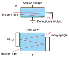
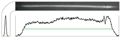
The KTN crystal we used had a thickness d of 1 mm and length L of 6 mm (of which the length of the interaction region was 5 mm). After depositing antireflection coatings on its light incident surfaces, we reflected light back into the crystal by placing mirrors close to its surfaces. In this way, we made a three-pass configuration. As the side view shows, the incident beam enters the crystal with a slight upward inclination, and after three trips through the crystal, it reaches the portion on the output surface that has no mirror and leaves as the emerging beam. A scan trace drawn by a deflected laser beam of wavelength λ = 633 nm on a screen placed on the output side is shown in Fig. 4. The beam was focused onto the KTN crystal with a spot diameter of 300 μm, and the applied voltage was varied in a range of ±350 V. As we expected, this arrangement tripled the deflection angle compared with the single-pass configuration, and the number of resolvable points was also tripled to become 61, as estimated from the length-to-width ratio of the trace.
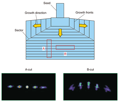
The reason we chose the multipass scheme is that in many circumstances it would be difficult to increase the length of the crystal. First, the KTN crystal sandwiched between electrodes constitutes a parallel-plate capacitor whose capacitance is proportional to its length. A large capacitance would increase the load on the driving voltage supply, which should preferably be avoided. The second reason, which is more specific to KTN crystal, is explained in Section 5. 5. Workaround for KTN crystal inhomogeneityA grown KTN crystal usually has some composition gradation along the growth direction. A composition variation manifests as a difference in phase-transition temperature Tc, which in turn causes a change in permittivity ε, leading to a larger change in Kerr constant that is proportional to ε2. In short, the performance of the KTN scanner is critically dependent on the composition variation. Let us examine the relevant crystal orientations. As shown in Fig. 5, the beam maintains a good pattern during deflection for orientation A, where the light beam travels through growth fronts. On the other hand, for orientation B, the composition variation on the incident surfaces causes the beam pattern to deteriorate when deflection occurs. As a result, orientation A is preferable, but it tends to include a less effective portion where Tc deviates further from the temperature at which the entire crystal is maintained, and hence where permittivity ε is smaller and eventually makes a smaller contribution to the EO effect.
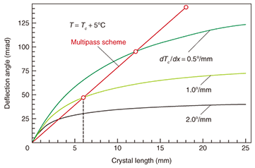
A model calculation of this situation is shown in Fig. 6. For orientation A, for three different dTc/dx values (assumed to be constant) along the crystal length L, the maximum deflection angle obtained for Emax = 600 V/mm was calculated as a function of L. For the initial relative permittivity εr, we assumed a value of 30,000. If the composition were not graded, the attainable deflection would increase linearly with length in a direction tangential to the curve at the origin. However, the composition variation causes a length increase to merely add inefficient parts, so the deflection angle does not increase but instead saturates. On the other hand, when the three-pass scheme is applied to, for example, a 6-mm-long piece of 1°/mm-quality crystal, the obtainable angle is simply linearly tripled compared with single-pass 6-mm chip. The result turns out to be far superior to what would be expected for an 18-mm crystal of the same quality. Thus, the multipass scheme, which achieves deflection equivalent to a longer crystal, is particularly beneficial in the case of KTN.
6. Prospects for resolutionWith the multipass scheme, if we increase the number of zigzags inside the crystal, could we increase the number of resolvable points indefinitely? Unfortunately, the answer is no. In addition to the constraint of Eq. (1), the maximum deflection angle is limited by an upper bound n (d - 2w)/L originating from the crystal’s aspect ratio. As the equivalent length L is increased by the multipass scheme, the deflection angle quickly reaches this limit, which suppresses further increases in N. In fact, we found that we could not obtain any further gains in resolution when we tried a five-pass configuration with the crystal described above. To further improve the resolution, we must either raise the geometrical upper bound by increasing the crystal thickness d or boost the number of resolvable points per length L by increasing the permittivity ε. The latter approach is especially promising because a steep increase according to ε2 is expected. For instance, if the relative permittivity εr is doubled to 30,000, we can expect to get 360 resolvable points, which rivals the resolution of current POS (point-of-sales) scanners. Thus, a large improvement in resolution can be expected with more homogenous crystals, which will be attainable through further refinements in the KTN growth technique. 7. ConclusionThe multipass scheme can enhance the resolution of a KTN scanner. We have already demonstrated a three-fold increase by using it. After assessing the factors that limit the resolution, we surmise that a large improvement is still possible by refining the compositional uniformity of the KTN crystal. References
|
||||||||||||||||||||||