|
|||||||||
|
|
|||||||||
       |
Special Feature: KTN Crystal Technologies Vol. 7, No. 12, pp. 27–31, Dec. 2009. https://doi.org/10.53829/ntr200912sf5 High-speed Spectrometer Using KTN Optical Beam ScannerAbstractThis article describes a spectrometer fabricated using a combination of a KTa1-xNbxO3 (KTN) optical beam scanner and a wavelength dispersion element. This spectrometer can measure a wide optical spectrum in microsecond-order time. A high-speed spectrometer is now being developed to observe ultrafast luminous phenomena. 
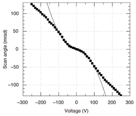
1. IntroductionA spectrometer is an instrument used to measure optical spectra. It can measure both the wavelengths and intensities of the target light. For example, it is used to evaluate the wavelengths of optical signals in optical communication systems such as wavelength-division multiplexing and also used to identify materials and their states by measuring the transmittance and/or reflectance of light. It basically consists of a wavelength dispersion element, a slit, and an optical detector. The wavelength dispersion element separates light spatially into components of different wavelengths. The specific wavelength of the separated light passes through the aperture of the silt and is detected by an optical detector. This is the basic concept for measuring the intensity of a specific wavelength. When the dispersion elements and the slit are fixed, only a fixed wavelength can be detected. On the other hand, optical spectra can be obtained dynamically as the wavelength passing through the slit is varied. One conventional way to change the wavelength passing through the slit is to rotate the dispersion element, which may be a prism or a diffraction grating, for example. However, physical rotation of the dispersion element limits the measurement speed. Another way to obtain optical spectra is to use an array of detectors instead of the slit-and-detector combination. This method has a complicated configuration, but it can measure wide optical spectra quickly. In this article, I describe the operating principle of a potassium tantalate niobate (KTa1-xNbxO3, KTN) optical beam scanner and a KTN spectrometer that utilizes it. The KTN optical beam scanner controls the wavelength to be measured and its wide scan angle and high-speed response make this spectrometer attractive. Before describing the spectrometer’s characteristics, I describe the scanning properties of the KTN optical beam scanner in Section 2. Then, in Section 3, I introduce the design scheme and describe practical operation of the KTN spectrometer. 2. KTN beam scannerA new phenomenon was discovered in 2005 using a KTN crystal. This beam-scanning phenomenon originates from the combination of space-charge-controlled electrical conduction and the electro-optic (EO) effect. The successful growth of large, optical-grade KTN crystals at NTT Photonics Laboratories has played an important role in making this discovery possible. Experimental results for scan angle versus applied voltage are shown in Fig. 1. The crystal temperature was kept in the paraelectric phase and the lowest-order EO effect was the quadratic Kerr effect. The crystal was cut and polished to a rectangular shape 6 mm long by 0.5 mm thick. A key requirement for the deflection phenomenon is the formation of an ohmic contact between the electrodes and the KTN crystal to produce a space-charge-controlled mode of electrical conduction. A uniform titanium electrode (length L = 5 mm) was deposited on both surfaces of the crystal. The light source was a linearly polarized He-Ne laser (λ = 638 nm), and the polarization was aligned with the electric field. When the voltage was changed from
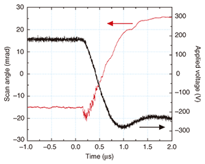
When the electrical conduction and electric field are controlled by the space charge, the electro-optically induced refractive index change is given by 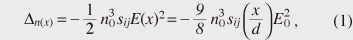 where n0 and sij are the refractive index and the Kerr constant of the crystal, respectively. Equation (1) indicates that the space-charge-controlled mode induces a linear gradient in the refractive index. As the optical beam propagates through the crystal, it is refracted by the linearly graded refractive index. For a paraxial beam, the deflection angle θ external to the crystal after the beam has traveled a distance equal to the interaction length L is given by 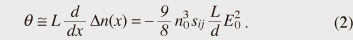 Here, the negative sign indicates that the beam is deflected toward the cathode. When the polarity of the applied voltage is reversed, the electrons are injected in the reverse direction and the beam is deflected with the opposite angle, giving a total deflection range of 2θ. My coworkers and I call this unique deflection effect the space-charge-controlled EO effect. In the experiment, the light polarization was aligned with the applied electric field, so the Kerr constant for this interaction was s11. The solid line in Fig. 1 is the theoretical fit obtained using Eq. (2) with sij = s11 = 1.0 × 10⁻¹⁴ m2/V2, n0 = 2.2, L = 5.0 mm, and d = 0.5 mm. It is a good fit with the experimental results. The value of s11 is a typical value that KTN exhibits at around the tetragonal-to-cubic transition temperature Tc [2]. The fact that the experimental results depart from the theoretical fit above 120 V and below -120 V could be due to saturation of the Kerr effect [2]. One of the attractive features of EO beam scanners is their high-speed scanning capability. We have confirmed the high-speed response of the KTN scanner. Figure 2 shows the response versus applied voltage (rectangular voltage at a repetition ratio of 100 Hz) and beam scanning angle for a 1-mm-thick KTN crystal. A scan time of 1 µs was obtained at the full scan angle of 45 mrad. The correspondence between measured scan response time and applied voltage means that the response was limited by our voltage circuit, so even faster scanning might be possible. For KTN, the EO effect itself is expected to have a frequency response of more than 500 MHz. We think that the response time is related to the transient behavior of the space-charge-controlled electrical conduction in addition to the frequency response of the EO effect. We are now investigating the transient behavior of the space-charge-controlled electrical conduction, which will be reported in future.
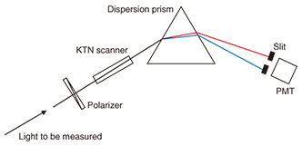
3. Design and performance of KTN spectrometer3.1 DesignThe spectrometer using the KTN optical beam scanner is schematically shown in Fig. 3. In our scheme, a polarizer and the KTN optical beam scanner are set in front of the wavelength dispersion element and the light passing through the slit is detected with a high-speed photomultiplier (PMT). The KTN optical beam scanner controls the angle at which light is incident to the wavelength dispersion element. The polarizer is used to align the light’s polarization with the electric field. Since the output angle from the wavelength dispersion element is determined by the wavelength and by the angle of incidence, the wavelength of light passing through the slit’s aperture is controlled by the scan angle of the KTN optical beam scanner. This spectrometer can measure a wide optical spectrum in microsecond-order time because of the fast scan response of KTN optical beam scanner.
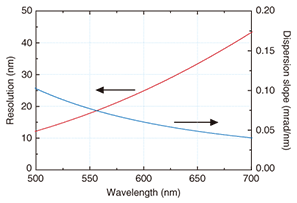
For a spectrometer, the important performance measures are resolution, sensitivity, measurable span, and so on. When the spectrometer uses the KTN optical beam scanner, they are mainly determined by the performances of the KTN optical beam scanner and the dispersion of the wavelength dispersion element. In this section, I describe an example of a KTN spectrometer using a standard-size KTN scanner and a BK7 glass prism. The KTN scanner is 6 mm × 5 mm × 0.5 mm in size. The beam diameter is 400 µm. The apex angle of the prism is 60°. The resolution and dispersion slope for this setup are shown in Fig. 4. The resolution indicates how well the spectrometer can separate the target light. The dispersion slope means the wavelength dependence of the output angle from the prism. The spectrometer’s resolution is determined by the beam diameter (divergence), the prism, and the slit, while the dispersion slope is determined by the material’s properties and incidence angle at the prism. When the beam diameter is large enough, the beam divergence is negligible, unlike for a conventional KTN scanner. In our configuration, I took into account the beam divergence. The resolution is high in the short wavelength regions and decreases with increasing wavelength because of the wavelength dependence of the beam divergence and the dispersion of the prism material. Once the dispersion angle has been determined by the material properties of the prism and the incidence angle, the required scan angle (change in incidence angle) is also determined. For this configuration, the required scan angle must be 0.75° (13.1 mrad). As shown in Figs. 1 and 2, the KTN optical beam scanner can meet this scan angle requirement. Moreover, higher resolution will be achieved by using a prism with greater dispersion. Furthermore, optimization of the KTN scanner size will improve the spectrometer resolution because the beam divergence increases in inverse proportion to the aperture size. However, there is a trade-off between aperture size and applied voltage because the beam deflection is parallel to the electric field rather than perpendicular to it as in the prism-type scanner.
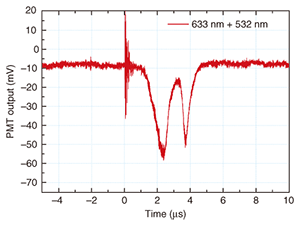
3.2 PerformanceI assembled the KTN spectrometer in accordance with the abovementioned design. Two different wavelengths of laser output were used to evaluate the measurement speed and resolution. The KTN optical beam scanner was driven with a rectangular voltage at a repetition ratio of 100 Hz. The applied voltage was changed from -250 to +250 V with a transition time of several microseconds. The measured optical spectrum of the laser output at both 532 and 633 nm (PMT output) is shown in Fig. 5. The two laser outputs were combined spatially and launched into the KTN optical beam scanner. They were spatially separated by the BK7 glass prism. As the KTN optical beam scanner changed the incidence angle to the prism, the wavelength passing through the fixed slit was changed. The PMT output peak around 2 µs is the signal of the 532-nm output while the peak around 4 µs corresponds to the signal of the 633-nm output. The spike around 0 µs is caused by the voltage applied to the KTN. This was confirmed to still exist as the KTN was driven even when there was no optical input. This spike can be reduced by using an electrical shield.
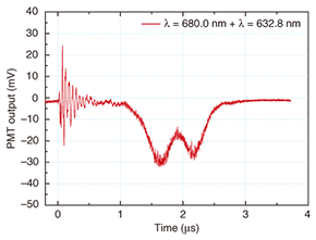
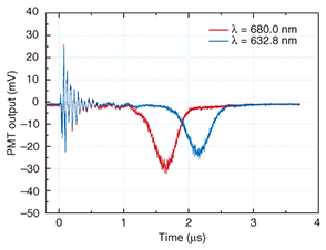
To evaluate the spectral resolution of this KTN spectrometer, two laser outputs with a wavelength separation of 47.2 nm were measured. The optical spectrum of laser output at both 680 and 632.8 nm is shown in Fig 6, where these two wavelengths are distinguished. This 47.2-nm wavelength separation is limited by the available lasers. The resolution at this wavelength was estimated to be 36 nm at the Rayleigh criterion. This result is in good agreement with the calculated value shown in Fig. 4. The two laser outputs were measured individually to double-check the resolution measurement result. Both results are plotted simultaneously in Fig. 7, where the red and blue lines are the results for 680 and 632.8 nm, respectively. The two peaks in Fig. 7 are at the same times as the peaks in Fig. 6. The longer wavelength signal appeared before the shorter wavelength signal. The spectrum in Fig. 5 has the opposite temporal relationship. It is possible to start measuring from either the short or long wavelength side because of the bilateral scanning characteristics of the KTN scanner.
4. ConclusionI introduced the operating principle of our KTN optical beam scanner and KTN spectrometer. Our KTN scanner can measure a wide optical spectrum in microsecond-order time. This spectrometer will be used to measure microsecond optical pulses, though continuous-wave laser inputs were used in the demonstration. The measured resolution of this spectrometer is in good agreement with the calculated value. Although I used visible wavelength in the spectroscopy demonstration, it is possible to scan the entire transparency range of the KTN crystal. The KTN scanner is expected to observe ultrafast luminous phenomena. References
|
||||||||