|
|||||||||||||||||||
|
|
|||||||||||||||||||
       |
Special Feature: Silicon Photonic Technologies Leading the Way to a New Generation of Telecommunications Vol. 8, No. 2, pp. 23–27, Feb. 2010. https://doi.org/10.53829/ntr201002sf4 Extremely-low-power-consumption Thermo-optic Switch with Silicon-silica Hybrid StructureAbstractIn this article, we introduce an optical switch with extremely low power consumption that unites the silicon photonic and silica-based planar lightwave circuit technologies developed at NTT Photonics Laboratory. 
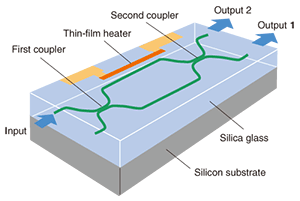
1. Energy consumption of optical communicationsAs the popularity of the Internet has increased, the amount of text, voice, and video transmitted has increased greatly. To handle this increase, the transmission capacity has been rapidly expanded by using wavelength division multiplexing (WDM), which multiplexes multiple optical carrier signals on a single optical fiber by using different wavelengths (colors). In the near future, when triple-play services (bundling telephony, Internet connection, and TV/video distribution) become common on fiber-to-the-home (FTTH) systems, metro or access layer networks are also expected to use WDM. In response to this further increase, networks composed of nodes such as reconfigurable optical add/drop multiplexers (ROADMs) and optical cross connects (OXCs) are beginning to spread. ROADM- and OXC-based networks require many optical switches to switch the destinations of light signals. However, these optical switches consume a lot of energy, which is a serious problem The energy consumption of the equipment used in a node increases as the traffic volume increases, and this has also become a problem in recent years. It is said that Internet growth will be limited by the required energy consumption even if there is sufficient space in the WDM bands [1]. Moreover, the amount of carbon dioxide released in generating the power used for optical communication throughout the world is reportedly more than the amount emitted by all the world’s aircrafts. The increase in the amount of traffic is a direct cause of the environmental problems that are currently a serious concern worldwide. In a word, we must develop a green optical switch that is both compact and inexpensive while consuming little energy. 2. PLC switches2.1 PrincipleA planar lightwave circuit (PLC) is a generic term used to refer to an optical circuit consisting of a light waveguide. In the same way as an electronic integrated circuit (IC), it is formed on the surface of a substrate using technologies such as thin-film formation, photolithography, and dry etching. Silicon is used as the substrate and silica glass as the waveguide. The merit of the PLC is that it provides a low-loss connection with optical fiber because the PLC and the optical fiber are both made of silica, and they both have a core size of the micrometer order. Optical switches are one of our main research topics. PLC switches have been installed in actual working nodes, and this has already helped to reduce costs, increase traffic capacity, and save energy in the optical network. We are currently developing various switches, including the two described below. They all use a Mach-Zehnder interferometer (MZI) as an element (Fig. 1). In this interferometer, the first coupler splits the input light into two (50:50 power ratio) and the second coupler merges them, which causes interference. When the switch is not driven, 100% of the light is output from output port 1 because this switch consists of a sequence of two 50% couplers. When we drive the thin-film heater and heat one waveguide, the light propagation speed in that waveguide decreases and the two lights are out of phase when they are merged in the second coupler, so the light is output from port 2. This is the operating principle of the MZI switch element. In a typical case, the time required to switch the output after power is supplied to the heater is only 2 or 3 ms.
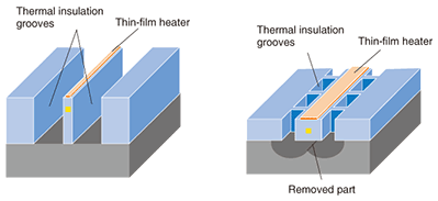
These structures have no moving parts, so they remain highly stable when subjected to vibration or impact. Silica is the main element found in such familiar objects as stones and window glass. An optical PLC switch made of silica has very high reliability and is capable of operating for tens of years without any deterioration in its characteristics. 2.2 Conventional approach to low power consumptionWe have already made low-power-consumption PLC switches by devising a structure based on a thin film heater [2], [3]. Figure 2 shows the area around the thin film heater shown in Fig. 1. To prevent thermal flow in the horizontal direction, thermal insulation grooves are formed near the thin film heater (Fig. 2(a)). In commercially available devices, the power consumption of one element is typically 100–200 mW (depending on the design), but at the research level it is already as low as 30 mW [2].
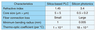
By using the additional devices shown in Fig. 2(b) to prevent thermal flow into the substrate, we can achieve even lower power consumption of 11 mW. This is very close to the value predicted by thermal simulation. In other words, we have already reached the lower power limit, and it would be very difficult to reduce the power consumption further using only silica material. 3. Silicon photonicsSilicon is an ideal semiconductor for electronic devices. Silicon photonics is a kind of PLC that uses silicon as a light waveguide instead of silica. In recent years, it has been actively researched because of its ease of integration with electronic devices such as ICs [4], [5]. The characteristics of a silica-based PLC and silicon photonics are compared in Table 1. In silicon photonics, the core cross-section is much smaller: the diagonal is less than 1 μm. One characteristic that requires careful attention is the refractive index. Si photonics can confine light well in a small core because silicon has a higher refractive index (3.4) than silica (1.46). This lets us make curved circuits with a small bending radius (~5 μm). Therefore, we can design optical circuits with the same configuration as silica-based PLCs, but about one hundred times smaller. Here, we should note that the thermo-optic coefficient of silicon is 18 times higher than that of silica. This means that the refractive index change needed for switch operation can be achieved by supplying less heat.
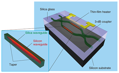
4. Silicon-silica hybrid PLC switchThis large thermo-optic coefficient makes possible a low-power-consumption optical switch. We have fabricated silicon-silica hybrid optical switches that only have silicon photonics embedded in a silica-based PLC (in the arm waveguides) to achieve low-power-consumption optical switches. A very important feature of our concept is that the device is not made entirely of silicon. By using a silicon-silica hybrid structure, we can retain the advantages of a PLC (namely low-loss connection to the fiber and high long-term stability) and obtain very practical switches with extremely low power consumption. A schematic of a developed silicon-silica hybrid optical switch consisting of an MZI is shown in Fig. 3. The inset shows a detailed view of the part of the silicon waveguide under the heater. The silicon waveguide has tapers at both ends. It acts as spot-size converter and connects the silicon and silica waveguides with low loss.
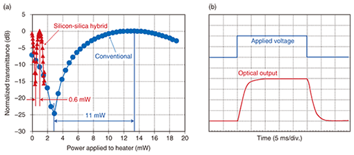
The measured switching characteristics of the silicon-silica hybrid PLC switch are shown in Fig. 4(a) and those of a conventional switch are also shown for comparison. The switching power (power consumed for transition between the on and off states) was only 0.6 mW, compared with 11 mW for a conventional switch. The ratio of these values (1/18) corresponds to the ratio of the thermo-optic coefficients of silica and silicon. This proves that we can successfully incorporate the physical properties of silicon into silica-based PLCs and achieve better power consumption than the current record. The measured time response of this switch is shown in Fig. 4(b). The time required to switch the output after power was supplied to the heater was 3.6 ms. This value is similar to that for a conventional silica-based PLC switch and is sufficient for use in ROADM or OXC nodes.
5. Concluding remarksThis silicon-silica hybrid optical switch will enable us to achieve dramatic energy savings because an optical switch can select an optical path freely. Our experimental results are the first fruit of uniting silicon photonics and silica-based PLCs. This combination retains the advantages of both technologies, and we can expect the functions of this hybrid switch to increase. We will continue to research and develop this boundary field of silicon photonics and silica-based PLCs to help increase communication capacity and overcome environmental problems. References
|
||||||||||||||||||