|
|||||||||||||||||||||
|
|
|||||||||||||||||||||
       |
Special Feature: Silicon Photonic Technologies Leading the Way to a New Generation of Telecommunications Vol. 8, No. 2, pp. 28–32, Feb. 2010. https://doi.org/10.53829/ntr201002sf5 Silicon-based Large-scale Photonic Crystal Nanocavity Arrays for Slow-light ApplicationsAbstractWe have developed a periodic array of photonic crystal nanocavities that acts as a slow-light waveguide with acceptable values of bandwidth and group velocity dispersion. The ultrahigh quality factor of 106 allows the array to couple 300 nanocavities, which delay an optical pulse by over 150 ps, which is more than thirteen times the original pulse width. 
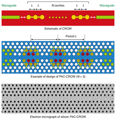
1. IntroductionSilicon-based electronics is the foundation of information technology and plays an essential role in our daily lives. Moreover, silicon is also a very attractive material for photonics. Like other semiconductor materials, silicon has a very high refractive index (~3.4) at the wavelength of 1.55 µm used as the optical fiber telecommunication band. As described in the other articles in this Special Feature, this high refractive index enables us to achieve a reduction of several orders in the size of optical integrated circuits compared with conventional silica-based technology. In addition, an advantage of silicon over other high-index semiconductor materials for the telecommunication band is its low material absorption that results from its relatively large indirect (electronic) bandgap. Thus, a low-loss waveguide [1] and a high-quality-factor (Q) optical cavity [2] have been made using silicon. The highly developed fabrication technologies for silicon electronics allow us to mass-produce submicrometer silicon photonic components on a 200- or 300-mm silicon wafer by photolithography. Its high index, low loss, and sophisticated fabrication technology also make silicon a good platform for photonic crystals (PhCs). For example, an optical cavity with a Q of over one million has been achieved only by using a silicon PhC [3]. Currently, the fabrication of high-quality silicon PhCs requires electron beam lithography, which is unsuitable for use in mass production. However, a silicon PhC has certain unique advantages over non-PhC-based silicon nanophotonics. The first is that we can make a nanocavity with a very high Q. The state-of-the-art confinement provided by a photonic bandgap can achieve a Q of over one million at the current level of fabrication accuracy (Q can theoretically exceed 108 under ideal conditions), which is one order of magnitude higher than that achieved with a silicon nanowire ring cavity [4]. A nanocavity can also achieve the net confinement of photons within a wavelength-sized volume, which is several orders of magnitude smaller than that achieved with a ring cavity. The very high Q per unit volume leads to cavity-based optical devices with an extremely low operating energy and greatly enhances light-matter interactions such as optical nonlinearity. The second advantage is the ability to slow down light. In a PhC, the group velocity and photon dispersion are determined by the photonic band structure, which depends on the PhC structure. Therefore, we can control the group velocity and dispersion by changing the design of the PhC. The slow light in a silicon PhC is also expected to enhance light-matter interactions. In this article, we report recent progress in silicon slow-light devices based on coupled PhC nanocavities. This provides an update to the Regular Paper in the Sep. 2009 issue [3], which reviewed in detail key technologies and principal experimental results related to this topic. Therefore, here we mainly discuss the PhC coupled cavity in terms of an on-chip silicon slow-light device and mention new record-breaking data obtained very recently by coupling 300 nanocavities [5]. 2. PhC coupled-cavity resonator arrayThere are several ways to achieve a slow-light waveguide on a PhC platform. A slow-light line-defect waveguide has the advantage of a relatively wide bandwidth, but it is difficult to slow light to less than 1/30 of its speed in a vacuum (c) with an acceptable loss at the current level of nanofabrication accuracy. An additional issue is the reduction in group velocity dispersion. Another way to achieve a slow-light waveguide on a PhC platform involves the use of a single ultrahigh-Q nanocavity for trapping light. This approach slows light the most, but there is no way to obtain sufficient bandwidth. To make a compact, low-loss, wide-bandwidth slow-light waveguide with small dispersion, which we believe to be essential for a usable device, we are focusing on a third way, namely the use of coupled cavities. A schematic of our PhC coupled-cavity array for slow-light applications (CROW: coupled resonator optical waveguide) is shown in Fig. 1. We used width-modulated line defect nanocavities, which have a Q higher than 106 [3]. According to a simple analysis [6], a CROW has a slow-light band with sinusoidal dispersion that gives it an acceptably low value of group velocity dispersion. We can control the speed of light in the material (here group velocity vg) by changing the coupling strength between cavities, which we mainly adjust by forming arrays with different periods (L). The bandwidth, namely the amplitude of the sinusoidal dispersion, is not restricted by Q. Since the scheme is applicable to any type of optical cavity, a large-scale CROW has also been developed in silicon ring cavities [4]. We believe that the PhC nanocavity is the best CROW platform on which to achieve an on-chip slow-light device because of its micrometer-order size (L = 2–5 µm, which is smaller than for any other cavities) and high Q of 106. Since current ring cavities have a Q of ~105 and a diameter of ≥10 µm, PhCs enable a more compact CROW with lower loss than a ring cavity and the same signal delay.
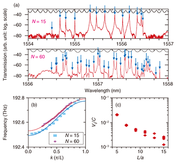
Experimental transmission spectra of the PhC-CROW are shown in Fig. 2(a). There are many discrete peaks corresponding to coupled resonator modes (CROW modes). We assigned every CROW mode n to a wavenumber k = (π/L)•n/(N+1), where N is the number of cavities in the array, and plotted the mode frequency as a function of the wavenumber (Fig. 2(b)). It is clear that the plots agree well with the ideal sinusoidal dispersion curve. Such a clear dispersion relation obtained by direct measurement of discrete CROW modes has been reported only for a PhC-CROW. The dispersion curve, which is directly combined with vg, can be controlled by changing L. The vg evaluated from the dispersion as a function of L is shown in Fig. 2(c). The results demonstrate that the CROW has the potential to achieve vg from c/50 to c/1000. The wide tunability of vg is an advantage of the PhC-CROW.
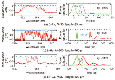
A transmission band consisting of discrete resonant modes, as shown in Fig. 2(a), is suitable for direct dispersion measurements (Figs. 2(b) and (c)) but unsuitable for light propagation. A different type of optimization yields a low-loss, wide-bandwidth CROW appropriate for practical devices. By maximizing the coupling between the CROW and the external waveguides, we obtained a wide flat passband, as shown in Fig. 3(a). For pulse propagation measurement, we used short pulses with a pulse width of 11–47 ps, which required a wide frequency bandwidth. Figure 3 also shows, for three different CROWs, the time-resolved signal after the pulse had propagated through the CROW. The shift of the peak with respect to the pulse propagating in the reference waveguide corresponds to the delay. As shown in Fig. 3(a), the delayed pulse that propagated via the CROW maintained its original shape well and the propagation loss was negligible. The transmission characteristics of the CROWs worsened as the length was increased (higher N) (Fig. 3(b)) or L was increased (Fig. 3(c)) owing to disorder among the cavities. Nevertheless, these CROWs still allowed a pulse to pass through with a large delay and acceptable loss, as shown in Figs. 3(b) and (c). When we consider that only a few years ago it was difficult even to form a CROW with ten cavities, we can appreciate what a great advance it is to have 300 cavities that are not only coupled together but also work fairly well as a slow-light waveguide. This is entirely because of the high Q value of 106. The delays of 35, 154, and 72 ps seen in Figs. (a)–(c) correspond to vg values of c/130, c/66, and c/170, respectively. The vg of c/170 is the lowest value measured directly in a dielectric waveguide. Thus, the vg in the PhC-CROW can be controlled relatively easily. As shown in Fig. 3, the CROW with vg of c/66 had the widest passband, so it successfully delayed a pulse with a small width of 12 ps. The ratio of the delay to the pulse width, which is regarded as the delay (shift) per bit, was approximately 13.
Currently, the performance of the PhC-CROW is greatly restricted by the disorder among cavities caused by fabrication error. If we can greatly improve the fabrication accuracy, we should be able to make a PhC-CROW with vg of less than c/500 that can delay an optical signal by more than a nanosecond with little loss and acceptable distortion. 3. ConclusionGreat progress has recently been achieved for silicon-PhC-based CROWs. Ultrahigh-Q PhC cavity technology has made it possible to couple 300 cavities, which was merely a dream a few years ago, and to achieve the net slowing down of a short optical pulse to a speed of c/170. We are continuing to develop the PhC-CROW because it is the only slow-light waveguide that simultaneously achieves vg less than c/30 and low propagation loss. The PhC-CROW has potential as an optical buffer memory and as a delay line. It is expected to greatly enhance optical nonlinear phenomena because of its very low vg. It is highly compact and ready for on-chip integration with other silicon nanophotonic devices and circuits. We hope that further progress in nanofabrication technology will make it possible to achieve low-cost mass production of PhC devices. References
|
||||||||||||||||||||