|
|||||||||||||||||
|
|
|||||||||||||||||
       |
Special Feature: Trends and Business Prospects for Human-area Networking Technology––Connecting People, Objects, and Networks Vol. 8, No. 3, pp. 13–18, Mar. 2010. https://doi.org/10.53829/ntr201003sf3 Modeling of Human-body Near-field Communication and Evaluation of Communication QualityAbstractIn this article, we describe the modeling of electric-field communication and the use of optical technology in the evaluation of an electric-field communication system. Using the model, we explain a basic principle of electric-field communication that uses the human body. The communication is susceptible to the effects of various types of noise from the environment, and the communication quality depends heavily on how it is used and on the installation environment. Since conventional measurement technology is unsuitable for precise evaluation of the quality, we introduced a novel optical measurement technique that enables precise evaluation because it does not affect the communication system. 
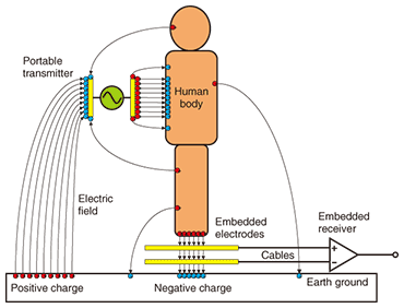
1. IntroductionHuman-body near-field electric-field communication technology lets you connect to a network through natural actions such as touching and stepping, so it is attracting attention as an innovative connection technology for person-to-person and person-to-object communication. Although it is well known that electricity easily passes through the human body, using the body like a cable is not that simple. The transmission path for electric-field communication has poor balance, so it is susceptible to the effects of various types of noise from the environment. Consequently, the communication performance depends greatly on the form of use and where the equipment is installed. To maintain stable communication, it is necessary to model a communication path that comprises the human body, a transmitter, a receiver, electrodes, and cables according to the form of use and then reflect it in the circuit design. Moreover, during the evaluation, the grounding condition can be easily changed by connecting the terminal to the measuring instrument, which can drastically affect the terminal’s state and lead to incorrect evaluation results. Correct evaluation of an electric-field communication terminal requires electrical isolation of the measuring instrument and the object being measured (device under test (DUT)). In this article, we describe the modeling of electric-field communication and the use of optical technology in the evaluation of an electric-field communication system. 2. Electric-field communication modelThe human body can be regarded as a conductor covered by skin, clothing, shoes, and other insulators [1]. Considering its size, the scale of the transmission path is about 1 m. Because the wavelength of a 10-MHz electrical signal is 30 m, for example, the transmission path of the electric-field communication can be considered to be sufficiently short relative to the signal wavelength. Accordingly, the transmission path can be treated as a lumped constant circuit for a megahertz-band electrical signal. Under such conditions, the spatial distribution of the electric field is similar to that of a static field around the transmission path. Such a field is also referred to as a quasi-static electric field. The model that we consider here is shown in Fig. 1 [2]. As a typical configuration, let us consider one-way communication from a portable transmitter to a receiver embedded in the environment (embedded receiver). The transmitter has two electrodes. When the electrical signal corresponding to the data to be transmitted is applied between the electrodes, an electric field is generated around the transmitter. The transmitter is placed in a pocket, in a bag, or on a neck strap, so it is always near the user’s body. The electric field generated by the transmitter creates an electric charge distribution on the body surface, which generates an electric field near the body. For signals with a frequency of 10 MHz or below, that field can be taken as a quasi-static electric field. It is thus distributed only in the vicinity of the body, in the same way as a static electric field, and not transmitted far like an electromagnetic wave. Accordingly, only objects extremely close to the human body can form an electric-field communication network. As we see in Fig. 1, the transmitter, human body, and earth ground are all linked by the electric field, forming a network. The embedded receiver detects the voltage generated between the embedded electrodes and thus receives the data signal from the transmitter.
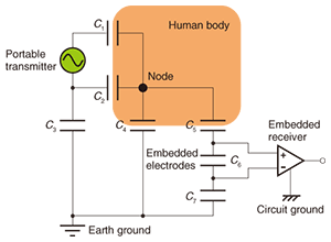
In this model, if we replace the parts where the electric field is generated with capacitors (C1 to C7), we obtain the equivalent circuit model shown in Fig. 2 [2]. The human body becomes a node in the circuit and is linked via capacitors to the transmitter and ground.
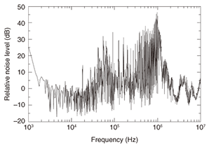
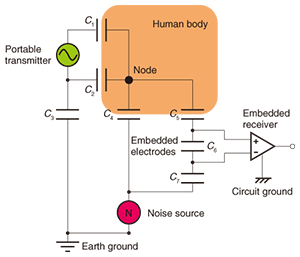
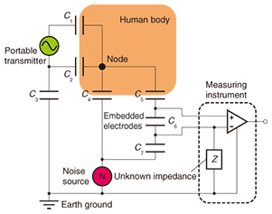
Noise electric fields are an important factor in electric-field communication. One particular problem is the noise electric fields produced by equipment power supplies, many of which are generated from floors and electrical outlets. These tend to be greater at low frequencies, so cell phones, which use gigahertz-band electromagnetic waves, are virtually unaffected by such noise electric fields. For electric-field communication using megahertz-band signals, however, such effects cannot be ignored. Noise electric fields from the floor affect the embedded electrodes to produce a noise voltage. An example of the spectrum of the noise level generated between the embedded electrodes is shown in Fig. 3. We can see that there is non-negligible noise even in the relatively high-frequency megahertz band. Since the embedded electrodes and the closest parts of the human body (the feet) are near the floor, they are strongly affected by noise originating there. On the other hand, the portable terminal is sufficiently far from the floor that the noise can be ignored in practice. An equivalent circuit model that takes into account noise electric fields from the floor is shown in Fig. 4.
Analysis of the equivalent circuit reveals that the quality of electric-field communication can be improved if the capacitance of each capacitor is optimized. If the shapes and sizes of the transmitting and receiving electrodes are appropriately designed to optimize the capacitances, some quality improvement is possible. In practice, however, the capacitances vary greatly with time and place and how the terminal is maintained. Obtaining stable communication quality, even after the capacitance values have been optimized, is one of the most important issues for electric-field communication. 3. Measurement and evaluation of electric-field communicationThe parameters of the equivalent circuit model of electric-field communication depend on various conditions, such as time and place. For that reason, in electric-field communication research and development, communication quality must be evaluated on the basis of correct measurements. Consider the case where an ordinary measuring instrument such as an oscilloscope or spectrum analyzer is used for measuring the signal generated between the embedded electrodes. The equivalent circuit model for when the measuring instrument is connected is shown in Fig. 5. In the figure, Z is an unknown impedance that depends on the measuring instrument. When the measuring instrument is connected, this unknown impedance is added between the connection point and earth ground, so the communication path that is measured is different from the original one. That is to say, the results obtained using an ordinary measuring instrument do not correctly reflect the original electric-field communication system signal and the noise.
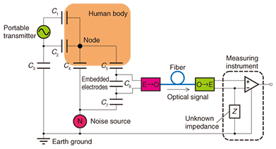
To achieve correct measurement, it is necessary to measure the signal with Z in Fig. 5 removed. We can eliminate Z by electrically isolating the DUT (embedded electrodes) from the earth ground and from the measuring instrument’s circuit ground. An effective way to achieve the desired electrical isolation is to use optical measuring technology [3]. The equivalent circuit model for an evaluation system using optical isolation is shown in Fig. 6. The device for converting the electrical signal (E) into an optical signal (O) is represented as E→O. Conversely, the device for converting the optical signal (O) into an electrical signal (E) is represented as O→E. The E→O device is connected to the DUT (embedded electrodes) and generates an optical signal that is proportional to the electrical signal generated between the electrodes. The optical signal propagates within the fiber to the O→E device, which converts it back into an electrical signal that can be used by the measuring instrument. What is important here is that the DUT is completely insulated from the measuring instrument by the fiber, thus eliminating the effects of unknown impedance Z and allowing correct signal measurement. The O→E devices are usually photodiodes. The E→O devices include active and passive types. The active ones include active components such as a light source, which are simple but do require a power source (e.g., battery). The passive ones consist of only passive components, such as an optical modulator, so such devices do not need a battery but do require light to be supplied by a fiber. To minimize the electrical effects on the DUT, one must choose a high-input-impedance E→O device. To obtain high input impedance, we mainly used a passive E→O device equipped with an electro-optical modulator [3].
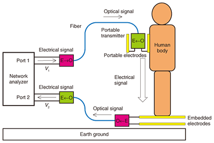
4. Systems for evaluating electric-field communication systemsAlthough the electric-field communication system can be replaced by an equivalent circuit, such as shown in Figs. 2 and 4, the capacitances included in the equivalent circuit (other than C6) vary with different conditions, so accurate measurement of the electric-field communication system characteristics is essential. An example of an evaluation system that uses optical measuring technology is shown in Fig. 7. For various frequencies, the network analyzer measures the ratio of signal V1 generated from port 1 to signal V2 detected at port 2 after passing through the body (V2/V1). It is isolated from the electric-field communication system by the fiber, so the characteristics of the transmission path, which includes the human body, can be correctly evaluated.
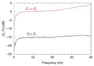
Some results obtained with the evaluation system shown in Fig. 7 are presented in Fig. 8. The frequency characteristics are relatively flat in the range from 2 to 40 MHz. Moreover, as expected from the equivalent circuit of Fig. 2, when C1 and C2 were balanced, the received signal was attenuated.
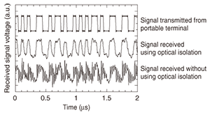
The benefits of optical measurement are shown in Fig. 9, which presents signal waveforms obtained with the measuring systems shown in Figs. 5 and 6. The upper waveform is the data signal waveform transmitted from the portable terminal. The middle waveform is the signal waveform received by the measuring instrument for a system of the type modeled in Fig. 6: it is similar to the upper waveform. The lower waveform is the signal waveform received by the measuring instrument for a system of the type modeled in Fig. 5. We can see that the high-frequency component is abnormally emphasized in the lower waveform, which was measured without the optical isolation and was thus affected by unknown impedance Z [2].
5. Future workWe believe that the electric-field communication system modeling and communication quality evaluation technique described here can be used at sites where equipment is actually to be introduced, as well as in communication device research and development laboratories. Facilitating the adjustment of onsite installations will lead to cost reductions and will ultimately accelerate the widespread use of this technology. In future work, we plan to continue to improve the modeling and evaluation technology with the aim of making a device that can be used for onsite testing. References
|
||||||||||||||||