|
|||||||||||||||||||||||||||||||||||||||
|
|
|||||||||||||||||||||||||||||||||||||||
       |
Letters Vol. 8, No. 8, pp. 38–43, Aug. 2010. https://doi.org/10.53829/ntr201008le1 40-km Single-mode-fiber Transmission for 100-Gbit/s Ethernet System Based on 25-Gbit/s 1.3-μm Electroabsorption Modulator Integrated with Distributed Feedback LaserAbstractWe have developed a 1.3-µm electroabsorption modulator integrated with a distributed feedback laser for medium- and long-distance 100-Gbit/s Ethernet. To ensure a sufficient extinction ratio in the 1.3-µm band, we used a tensile-strained quantum well absorbing layer made with InGaAlAs-based material, which has a larger conduction band offset than InGaAsP. The modulator was coupled to the laser by butt jointing to optimize the structure separately. The fabricated device packaged in a butterfly module has a small-signal 3-dB bandwidth of 33 GHz. With this module, we demonstrated 10- and 40-km transmission on a single-mode fiber at the modulation speed of 25 Gbit/s at 40°C. 
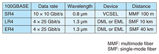
1. IntroductionLightsources for 100-Gbit/s Ethernet (100GbE) [1] have been intensively studied recently for the construction of the next-generation network. In 100GbE, various standards have been discussed for different transmission distances. For optical fiber transmission, three standards called 100GBASE-SR4, -LR4, and -ER4 are defined (SR: short reach, LR: long reach, and ER: extended reach), as listed in Table 1. For short-distance transmission (SR4, 100 m), 0.8-µm 10 × 10-Gbit/s lightsources are required for multimode fiber transmission and vertical cavity surface emitting lasers (VCSELs) are used. For medium-distance transmission (LR4, 10 km) and long-distance transmission (ER4, 40 km), 1.3-µm 4 × 25-Gbit/s lightsources are required for single-mode fiber transmission. In these standards, some specifications for lightsources are defined, such as, side mode suppression ratio (SMSR) > 30 dB and dynamic extinction ratio (DER) > 4 dB (LR4) and > 8 dB (ER4).
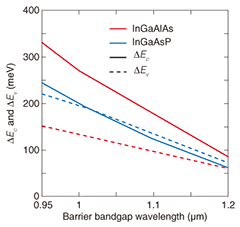
Directly modulated lasers (DMLs) [2]–[5] and electroabsorption modulators integrated with distributed feedback lasers (EMLs) [6]–[9] are promising candidates and have been developed mainly for the LR4 system. Although DMLs are more compact, easier to fabricate, and more energy-efficient than EMLs, chirp is an inevitable problem because of the refractive index fluctuations associated with the modulation. Furthermore, it is hard to obtain the large extinction ratio required for the ER4 system. EMLs are larger than DMLs and need an additional electrode to operate the laser diode (LD) and the electroabsorption modulator (EAM), resulting in higher power consumption. However, the layer structures of the LD and EAM can be optimized separately, and it is easier to obtain a larger extinction ratio and to manage the chirp than with DMLs. In particular, for the ER4 system, EMLs are almost indispensable because of the high extinction ratio requirement. In this work, we have developed a 1.3-µm EML for the LR4 and ER4 systems and demonstrated 10- and 40-km error-free transmissions on a single-mode fiber under 25-Gbit/s operation. The device is a promising candidate for long-reach 100GbE. 2. Device design and fabrication2.1 Material and quantum well designFor the EAM, we used an InGaAlAs-based tensile-strained multiple quantum well (QW) to ensure a large extinction ratio. The InGaAlAs-based QW provides a larger conduction band offset ΔEc than an InGaAsP-based QW [10]. The ΔEc and valence band offset ΔEv of 1.3-µm QWs are shown in Fig. 1 as a function of the bandgap wavelength of barrier materials. The ΔEc of the InGaAlAs QW is several tens of millielectronvolts larger than that of the InGaAsP counterpart. Therefore, the wavefunction leakage to the barrier region is small and the wavefunction overlap between the conduction and valence bands is large under the bias electric fields, leading to a large extinction ratio. It should also be noted that since the ΔEv of an InGaAlAs QW is smaller than that of an InGaAsP QW, the hole-pile-up effect that occurs under modulation can be suppressed.
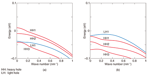
Typical valence band structures of compressive- and tensile-strained QWs are shown in Figs. 2(a) and 2(b), respectively. For compressive-strained QWs, the first valence subband is heavy-hole-like. If the strain is increased, the energy separation between the first and second valence subbands becomes large [11], [12]. In this case, the density of states around the top of the valence band is decreased, resulting in a small absorption coefficient. In the case of tensile-strained QWs, the first and second valence subbands are light- or heavy-hole-like. We can make the energy separation between these bands very small by adjusting the strain, as shown in Fig. 2(b). Therefore, the density of states around the top of the valence band is increased and the absorption coefficient becomes large. It should be noted that the momentum matrix element of the transition from the conduction band to the light-hole band is one-third that of the conduction-band-to-heavy-hole transition.
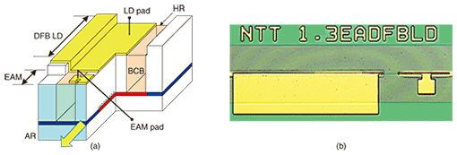
2.2 Optical waveguide designFor QW semiconductor devices, buried waveguide structures in which both sides of the active region are buried with semiconductor cladding layers have been used. Although this structure provides high current injection efficiency and a circular beam profile, the modulation bandwidth is limited owing to the large dielectric constant of semiconductors. To obtain the large electrical-to-optical conversion (E/O) bandwidth required for 25-Gbit/s operation, a ridge-type waveguide structure is used. Burying both sides of the ridge with a low-dielectric-constant polymer makes the parasitic capacitance small, leading to a large E/O bandwidth [13], [14]. Moreover, butt-joint coupling is used to connect the LD and EAM to optimize their structures separately. 2.3 Device fabricationThe structure of our EML is schematically shown in Fig. 3. The QW structures of the LD and EAM were grown by metalorganic vapor phase epitaxy. After the ridge waveguide had been formed, both sides of the ridge were buried with benzocyclobutene (BCB). Bonding pads were evaporated on top of the LD and EAM. Anti-reflection and high-reflection films were coated on the front (EAM side) and rear (LD side) facets. The fabricated chip was mounted on a chip carrier and packaged in a butterfly module. A photograph of the fabricated chip is shown in Fig. 3(b).
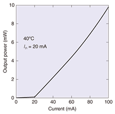
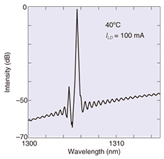
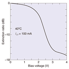
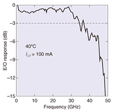
3. Device performanceThe optical output power of the fabricated chip as a function of injection current is shown in Fig. 4. All the measurements reported in this article were done at 40°C. The threshold current was 20 mA. Optical output of about 10 mW was obtained with an injection current of 100 mA. The lasing spectrum obtained with the 100-mA injection current is shown in Fig. 5. The lasing wavelength was around 1305 nm with an SMSR larger than 40 dB. As shown in Fig. 6, the static extinction ratio (SER) was over 16 dB. The detuning between the lasing wavelength and the EAM band-edge was adjusted to obtain a sufficient extinction ratio at 40°C to reduce the module’s power consumption. The small-signal E/O response is shown in Fig. 7. The injection current to the LD was 100 mA. The 3-dB bandwidth was 33 GHz, which is sufficient for 25-Gbit/s modulation. Moreover, the temperature dependence was almost negligible.
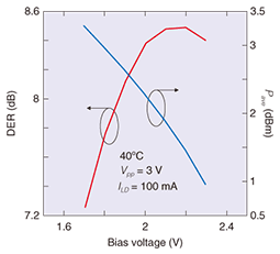
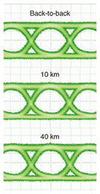
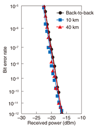
Using the device, we performed a 10- and 40-km transmission experiment on a single-mode fiber at 40°C. A 25.78125-Gbit/s, non-return-to-zero, 231-1 pseudorandom bit sequence signal was used. The DER and average output power Pave as a function of the modulator bias voltage are shown in Fig. 8. The injection current to the LD was 100 mA, and the voltage swing Vpp was 3 V. For a larger bias voltage, the DER became large since the light was modulated in the steep region of the extinction ratio curve (Fig. 6). Here, to achieve 8-dB DER, which is required for ER4, the bias voltage was set to 1.9 V. In this case, the DER was 8.2 dB and Pave was 2.6 dBm. Non-filtered eye-diagrams obtained for the back-to-back configuration and obtained after 10- and 40-km transmissions are shown in Fig. 9. Clear eye-openings can be seen even after 40-km transmission. The back-to-back bit-error-rate performances after 10- and 40-km are shown in Fig. 10. The power penalty was almost negligible, and error-free operation up to 40 km was successfully demonstrated.
4. ConclusionWe have developed a 1.3-µm InGaAlAs-based EML for a high-speed next-generation network. Tensile-strained QWs and a ridge waveguide structure were used to obtain a large extinction ratio and a large E/O bandwidth. Error-free transmission up to 40 km on a single-mode fiber under 25-Gbit/s operation was demonstrated. These results indicate that our device is a promising lightsource for metro-area 100GbE. References
|
||||||||||||||||||||||||||||||||||||||