|
|||||
|
|
|||||
       |
Special Feature: Front-line Materials Research Vol. 8, No. 8, pp. 5–6, Aug. 2010. https://doi.org/10.53829/ntr201008sf1 Materials Research ActivitiesAbstractNTT Laboratories performs materials research because it plays a fundamental role in the development of information and communications systems. This Special Feature introduces our work on four materials: aluminum nitrides, diamond, graphenes, and nanowires. The research is proceeding in three directions: composition control, high crystal quality, and low dimensionality. 
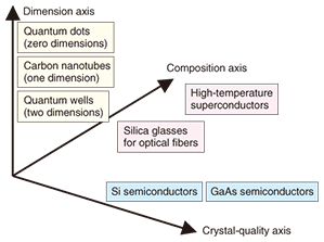
1. IntroductionSince the earliest times, human society has made progress by using and developing various materials. NTT Laboratories has been performing materials research because it plays a fundamental role in the development of information and communications systems. We have created materials that have had a great impact on society such as semiconductor crystals and glass for optical fibers. We are currently researching materials with useful functions for overcoming future social problems. In this Special Feature, we introduce our work in four areas of materials research: (1) aluminum nitrides for environmental and sanitation applications utilizing high-efficiency deep-ultraviolet light emission, (2) diamond for high-frequency power devices with very low energy consumption, (3) graphenes, which are two-dimensional materials consisting of carbon atoms that are expected to form next-generation electronics materials, and (4) compound-semiconductor nanowires, which are one-dimensional materials, for controlling single electrons and single photons. 2. Three materials research directionsThe status of these four materials research areas can be understood by considering the directions being taken in the research. As shown in Fig. 1, three directions are being followed with a view to creating new materials.
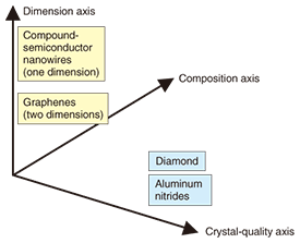
The first direction is composition control where the goal is to synthesize novel materials such as high-temperature superconducting copper-oxide materials. This work also involves creating new characteristics by minimizing the impurity content. Examples include silicon single crystals and silica glass materials for optical fibers. The second direction is high crystal quality. In some cases, crystals with no polycrystal area and a very low defect density are needed if we are to obtain useful functions. Examples of this work include silicon single crystals used as substrates for large-scale integrated circuits (LSIs), which are also examples of work in the composition direction. The movement of electrons and holes, which is very important for semiconductor functions, is hindered by many polycrystal areas or a high density of defects. Crystal growth has been researched for silicon single crystals, and silicon single crystals have been made with no polycrystal areas, minimal defect densities, and large sizes. LSIs made of these crystals support today’s society. Similarly, gallium-arsenide and indium-phosphide single crystals with low defect densities have been made, and they are used as semiconductor laser materials. Thus, one aspect of crystal quality research is the study of crystal growth techniques. Another type of crystal quality research is focused on doping techniques. Two states, namely the positive (p-type) and negative (n-type) states, are required if we are to use semiconductor characteristics effectively. Impurity atoms are deliberately injected into semiconductors to make p- or n-type states. Research on effective doping techniques for maintaining crystal quality is very important. The third direction is low dimensionality. Ordinary materials have three-dimensional structures and exhibit corresponding characteristics. The characteristics of zero-dimensional (point), one-dimensional (line), and two-dimensional (plane) structures are quite different from those of three-dimensional structures. For example, light emission efficiency and electron conductivity both increase. Quantum-well structures (two-dimensional structures) and quantum-dot structures (zero-dimensional structures) applied to laser diodes are examples of this third research direction. In addition, carbon nanotubes have been studied as one-dimensional materials. For low dimensionality, control of the sizes and densities of low-dimensional structures is very important. 3. Problems to be solvedOf the four materials introduced in this special feature, research on aluminum nitrides and diamond is concerned with high crystal quality, and research on graphenes and nanowires is concerned with low dimensionality, as shown in Fig. 2. There are various problems to be solved in relation to materials research. Aluminum nitrides, which have the advantage of possessing the shortest light emission wavelength among semiconductor materials, face problems with crystal quality and doping. Diamond, which has the advantages of very high dielectric strength and very high thermal conductivity, also faces problems related to crystal quality and doping. Graphenes, which have the advantage of very high electrical conductivity, face issues regarding the formation of large-area thin films and the theoretical prediction of characteristics for applications. Nano-wires, which offer the advantages of high electron and photon controllability and good crystal quality, require further investigation of ways to fabricate composite structures using materials with different compositions. This Special Feature introduces NTT’s research approaches for overcoming these problems.
|
||||