|
|||||||||||||
|
|
|||||||||||||
       |
Special Feature: Front-line Materials Research Vol. 8, No. 8, pp. 12–16, Aug. 2010. https://doi.org/10.53829/ntr201008sf3 Diamond Field-effect Transistors as Microwave Power AmplifiersAbstractThis article reviews the present status and future prospects of diamond transistors for microwave power amplifiers. NTT has been developing a technology for growing high-quality diamond film and has successfully fabricated diamond field-effect transistors (FETs) using the film. These diamond FETs exhibit the highest reported frequency limit in the millimeter wave range and the highest reported radio-frequency power capability in the microwave range. 
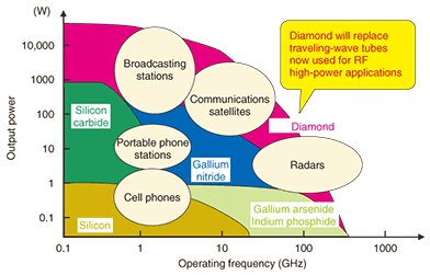
1. IntroductionThe data transfer rate in communications is increasing very rapidly. Therefore, electronic devices that operate at higher frequencies and generate higher output power are urgently needed for the present and future communications systems. On the other hand, from the environmental and energy-saving viewpoints, higher power efficiency from semiconductor devices is required at the same time. Diamond semiconductor will satisfy all of these requirements. The output power and operating frequency currently required for some specific applications and the performances of devices made from various semiconductors are shown in Fig. 1. Cell phones require an output power of ~0.9 W and a frequency of ~0.9 GHz and use silicon (Si) or gallium arsenide (GaAs) power amplifiers. GaAs power amplifiers are currently used as power amplifiers in base stations, but gallium nitride (GaN) has recently made inroads in this area. Silicon carbide (SiC) has progressed as a material for power devices, but the operating frequency of SiC-based devices will be limited to 1 GHz because of its low carrier mobility. On the other hand, broadcasting stations, communications satellites, and radars require higher output powers and frequencies, for example, 120 W and 10 GHz, respectively, for communications satellites. Such performance is beyond the ability of conventional semiconductor devices, so these applications still rely on traveling-wave tubes, which are vacuum tubes. However, the power efficiency of vacuum tubes is low because a large proportion of their input power is consumed as heat. Therefore, from the environmental and energy-saving viewpoints, vacuum tubes should be replaced by semiconductor devices.
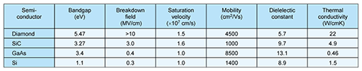
Diamond is called the ultimate semiconductor because it intrinsically has many superior physical properties over conventional semiconductors. As listed in Table 1, diamond’s band gap is five times as wide as Si’s, which means that diamond’s breakdown field is 30 times higher; consequently, the output bias voltage can be set to the same ratio. As power is the product of voltage and current, the available power can be increased. Furthermore, the electron mobility in diamond is three times as high as in Si, which means that the device’s on-site resistance, or power consumption, during operation can be reduced. As is widely known, diamond has the highest thermal conductivity among all known materials, so it has the highest heat-dissipation efficiency during high-power operation. Therefore, a diamond device’s temperature rises much less for a specific power consumption. Diamond’s drift velocity is similar to that of GaAs; therefore, diamond transistors will exhibit high radio-frequency (RF) power capability, like GaAs transistors.
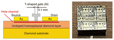
2. Diamond FET fabricationAs explained above, the physical properties of diamond are excellent for achieving high-frequency, high-power, high-efficiency RF power amplifiers. However, diamond crystal is extremely hard, and until recently the high-purity diamond crystals needed for semiconductor devices were extremely difficult to grow. Utilizing our long experience in high-purity semiconductor growth, my coworkers and I have clarified the crystalline-defect-formation mechanisms in diamond and reduced the defect-density by one order of magnitude. We have also reduced the concentration of impurities, such as nitrogen, and developed technology for growing high-quality diamond thin films [1]. After these successes, we moved on to the development of diamond device fabrication technology, which requires p- and n-type diamond. For the doping, we developed an ion-implantation technology that increases the doping efficiency by one order of magnitude. Below, we describe how we use hydrogen (H) surface termination as a doping method. A photograph of an entire sample (3 mm × 3 mm) and a cross-section drawing are shown in Fig. 2. Field-effect transistors (FETs) are fabricated on high-purity diamond crystal. When H atoms are chemically adsorbed onto diamond surface, a two-dimensional hole channel is formed along the surface for a few nanometers. Gold (Au) is evaporated for source and drain contacts. The gate length decreases the time it takes carriers to run below the gate, so the transistors can operate at a higher frequency. For the fabrication of submicrometer gates, we use electron beam lithography.
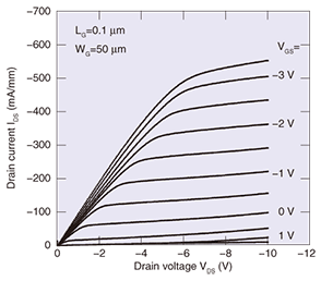
3. Characteristics of diamond FETThe DC drain current-voltage (I-V) characteristics (output characteristics) of a diamond FET with a gate length of 0.1 μm are shown in Fig. 3. We obtained the maximum drain current of 0.55 A/mm [2], which satisfies demands for practical use.
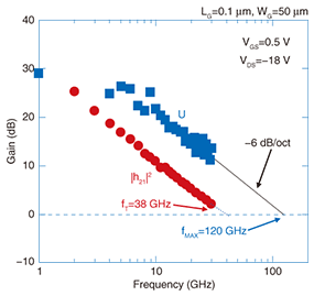
The RF small-signal characteristics—frequency dependence of current gain (|h21|2) and power gain (U) —of diamond FET [2] are shown in Fig. 4. The maximum oscillation frequency (fMAX), the upper limit of the operating frequency in power amplification, is 120 GHz. This cut-off frequency is the highest ever reported for diamond devices. These results were the first demonstration showing that diamond FETs can operate as amplifiers in the millimeter-wave (30–300 GHz) range.
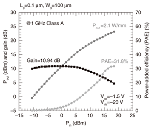
The input-output power characteristics (large-signal characteristics) of the diamond FET in the class-A operating condition at 1 GHz [3] are shown in Fig. 5. The maximum power level PMAX was 2.1 W/mm, the linear gain was 10.94 dB, and the power-added efficiency was 31.8%. This is the highest PMAX among diamond devices and it is twice that of conventional GaAs power amplifiers. This indicates the suitability of diamond RF power amplifiers for communications systems.
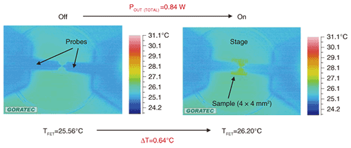
The increase in device temperature during RF power operation monitored by infrared thermography [4] is shown in Fig. 6. During powered operation (right), at a power consumption of 0.84 W, the device temperature increased by only 0.6°C. This temperature rise is only 1/50 of that for GaAs transistors. Physically, the temperature rise should be inversely proportional to the thermal conductivity. Since the thermal conductivity of diamond (22 W/mm) is 50 times as high as that of GaAs, this experimental result is very reasonable. From the viewpoint of thermal management, which is very important in power device circuit design, this is a very interesting result.
4. ConclusionThe present status of diamond device research in NTT was described. When diamond devices are established, they will considerably improve the capabilities of information and communications technology (ICT), which will in turn lead to improved energy efficiency. NTT has clarified the p-type doping mechanism and improved device properties, reliability, and ion implantation technology. We are working hard to develop basic technologies for making diamond devices. References
|
||||||||||||