|
|||||||||||||||||||
|
|
|||||||||||||||||||
       |
Feature Articles: System LSI Design for Broadband Optical Access Network Systems Vol. 9, No. 3, pp. 23–28, Mar. 2011. https://doi.org/10.53829/ntr201103fa4 Design Verification Using Field-programmable Gate Arrays for Optical Access Communications SoCAbstractWe describe evaluation technology that uses field-programmable gate arrays (FPGAs) to test a system on a chip (SoC). This should reduce the time taken for testing SoCs used in optical access communications by letting us conduct tests using FPGAs in parallel with conventional testing to reduce the testing time and improve the design quality. 
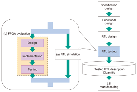
1. IntroductionThe process of evaluating a system on a chip (SoC) involves verifying a register transfer level (RTL) description. The RTL description is written in a hardware description language and created through specification design, functional design, and RTL design, as shown in the SoC design flow in Fig. 1. The result is a verified RTL description, called a clean file, which is used next in the large-scale integrated circuit (LSI) production process.
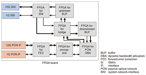
SoC evaluation usually takes several times longer than SoC design, so as the scale of designs increases, the evaluation time is becoming a problem. Moreover, if a problem is discovered during the evaluation, the evaluation process can take even longer because additional checking is needed after the problem has been fixed to ensure that revisions have not affected other aspects of the design. Furthermore, the repair time and cost for fixing problems found after production has begun can be very high, so as much testing as possible must be done to eliminate these problems beforehand. To date, SoC testing has generally been done using a logic simulator, which is a computer program ((a) in Fig. 1). However, simulating the functions of a large-scale device such as an SoC takes a long time, which makes it difficult to test all of the functionality adequately. 2. Benefits of FPGA testingTo overcome this problem with logic simulation, it has recently become more common to conduct testing using field-programmable gate arrays (FPGAs) ((b) in Fig. 1) in parallel with logic simulation. An FPGA is an LSI [1] that can be programmed any number of times for the desired logic. In FPGA testing, hardware with the same functionality as the SoC is implemented by writing FPGA design data to an FPGA mounted on an evaluation board. This data is created from the hardware description of the SoC design. The functionality is then checked using measuring instruments to input data and evaluate whether the intended output data is obtained. FPGAs can operate several hundred times faster than a logic simulator, so they make possible long-term, continuous testing that is difficult with simulation. Functionality can also be evaluated under conditions closer to real ones by connecting the evaluation board to other equipment and communicating at real speeds. FPGA evaluation allows functionality to be tested under more conditions than logic simulation and thereby allows for more improvements in design quality. Another major benefit is that in combination with software, overall system operation can be tested. In this article, we focus on RTL evaluation using FPGAs. 3. Features of FPGA testing for optical access communications SoCsThis type of FPGA testing has many benefits, but when used to test SoCs for optical access communications, it must support large-scale systems and high-speed communications and make the test shorter and easier to perform. Below, we describe how these issues are handled. 3.1 Large-scale systemsAn optical-access communications SoC requires a variety of functions, from communications using the prescribed protocol, to encryption for maintaining security and quality-of-service control to maintain service quality, so the design data may be large-scale. For testing, the design data must be written to FPGAs, but a large-scale design may not fit onto a single FPGA device. In such cases, the design data can be divided and written to multiple FPGAs, but this presents the additional issues of how to divide the design data appropriately and how to transmit high-speed signals among the devices. Communications SoCs are usually organized to perform the prescribed processing in order according to the signal flow for upstream and downstream signals. Thus, the design can be divided according to the major functions to enable this sort of processing, and each function can be implemented in a separate FPGA (Fig. 2).
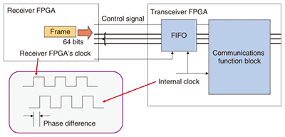
3.2 High-speed communicationsThe next-generation of optical access communications SoCs will send and receive data at a high wirespeed of 10 Gbit/s. FPGA testing allows the design to be evaluated at these speeds, so this technology has the advantage of evaluating the design under nearly real conditions. When data is transmitted among multiple FPGAs, it can be difficult to transmit or receive data between devices in some cases owing to delay in the lines among FPGAs or to phase differences among the FPGA clocks. For this reason, in 10-Gbit/s processing, a 64-bit-wide data frame and control signals are sent together with the clock from the sending FPGA to the receiving FPGA (Fig. 3). The data is written to a first-in first-out (FIFO) buffer in sync with the sending FPGA’s clock. It is then read out of the buffer in sync with the receiving FPGA’s clock to compensate for any phase differences and to maintain high-speed communications [2].
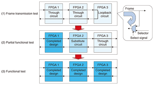
The wiring, connectors, and other aspects of the FPGA evaluation board are also selected to handle high-speed communications. 3.3 Reduced testing timeFor large-scale SoCs, all the functional blocks are designed and tested in parallel. With conventional FPGA testing, frame continuity is not achieved, and it is impossible to test all functional blocks or the LSI as a whole until the design data for all functional blocks has been implemented in FPGAs. Because of this, if the design and testing of a particular block is delayed and the block has not yet been implemented in the FPGA, testing cannot begin, which creates a bottleneck for the entire test schedule. To deal with this issue, various approaches are used to replace the FPGA that is behind schedule until it is ready in order to prevent major delays in the overall test schedule. These include using an FPGA that implements only the minimum functionality (a substitute circuit), one that simply takes a frame from the previous block and outputs it in a format acceptable to the following block (through circuit), and one that takes the output from the previous block and sends it back as input to the previous block (loop-back circuit). Examples of applying these types of circuit at various stages of testing (gradual FPGA testing method) are shown in Fig. 4. In the early stages of testing, none of the block designs are complete, so a through circuit is implemented for each one and a loop-back circuit is used to perform a frame continuity test (1). When the designs of some of the blocks are complete, either through or substitute circuits can be used for blocks that are still incomplete so that FPGA testing of the completed circuits can proceed (2). In this way, evaluation can proceed, starting with the blocks completed first, and at the end, when the designs and FPGA implementations for all blocks are complete, the overall LSI functionality is tested (3). Before the designs for all of the blocks are complete, testing of individual functional blocks can proceed (1)–(2), and when the design data for all of the blocks is ready, testing of the overall LSI is done. This allows testing to be completed earlier than with previous approaches.
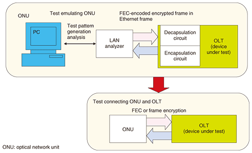
3.4 Easier testingAn SoC for communications processes frames from the communications path, performing forward error correction (FEC) to correct errors, encryption to provide high security, etc. Testing instruments similar to local area network (LAN) analyzers are used in FPGA testing for communications SoCs, but they generally cannot create or receive these types of frames, so it is impossible to check functionality without performing testing by actually connecting together devices of the same type. To resolve this issue, we built the test system shown in Fig. 5.
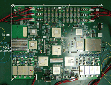
This system consists of a LAN analyzer that embeds test data generated on a personal computer (PC) in frames and sends them to the FPGA port, and an optical line terminal (OLT) FPGA board (see “MAC LSI Design Technology for Optical Access Communications” [3]) with the circuit being tested as well as circuits that encapsulate and decapsulate the test data from the frames and send them to the test circuit. Test frames are encrypted and FEC-encoded using a program running on the PC, stored in the data segments of Ethernet frames by the LAN analyzer, and input to the OLT FPGA board. On the FPGA board, the decapsulation circuit retrieves the encrypted and FEC-encoded frames from the Ethernet frames and removes the FEC encoding and encryption. Correct operation can be checked by comparing the test frame with the output frame. This method makes tests simulating communication conditions easy to do using an ordinary LAN analyzer. 4. FPGA evaluation boardsAn example of an FPGA evaluation board developed for an optical access communications SoC is shown in Fig. 6. This evaluation board implements OLT circuits in multiple FPGAs for FPGA testing.
5. Future developmentsAfter an LSI has been produced, an LSI evaluation board is constructed and the LSI’s system operation is tested. FPGA testing know-how can also be useful for this. We plan to study new functionality by using the fact that functions on the FPGA board itself can also be modified. References
|
||||||||||||||||||