|
|||||||||||||||||||||||||||
|
|
|||||||||||||||||||||||||||
       |
Feature Articles: System LSI Design for Broadband Optical Access Network Systems Vol. 9, No. 3, pp. 29–35, Mar. 2011. https://doi.org/10.53829/ntr201103fa5 10-Gbit/s Burst-mode Receiver Integrated Circuits for Broadband Optical Access NetworksAbstractWe introduce burst-mode receiver integrated circuits that can respond instantaneously to a suddenly arriving optical signal and receive it correctly. They are suitable for the next-generation optical access system (10G-EPON: 10-Gbit/s Ethernet passive optical network), which requires a receiver that can receive high-speed (10-Gbit/s) optical burst signals, unlike typical receivers which receive continuous signals. 
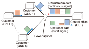
1. IntroductionNTT’s FLET’S Hikari service, which is a passive optical network (PON) system, is currently spreading in Japan. In this service, the signal sent from a customer’s terminal (optical network unit (ONU)) to the optical line terminal (OLT) in the central office is a burst signal. Unlike the continuous signals widely used with Ethernet and other technologies, burst signals have no signal at all between data segments. Moreover, the distances from customers to the central office vary, which affects the signal strength accordingly. This is shown in Fig. 1, where the signal from ONU 1 is strong, while that from ONU 2 is weak. For the central office to be able to handle such customer data, these optical burst signals with differing strengths and timings must be converted into electrical signals of fixed intensity and timing. For the next generation of optical access communications, this functionality must be achieved for data being transmitted at ten times the current speeds.
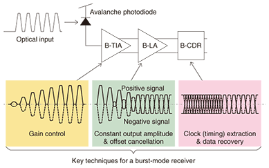
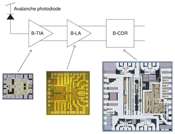
2. Receiver architectureAs shown in Fig. 2, the burst-mode receiver [1], [2] for an OLT consists of an avalanche photodiode, which converts the optical signal into an electrical current signal; a transimpedance amplifier (TIA), which amplifies and converts the current signal into a voltage signal; a limiting amplifier (LA), which converts weak and strong voltages into fixed-amplitude voltage signals; and a clock and data recovery (CDR), which extracts the timing clock from this signal and reshapes the signal waveform using the extracted clock signal. For a burst-mode receiver, the TIA, LA, and CDR need to be burst-mode devices, which are denoted B-TIA, B-LA, and B-CDR, respectively.
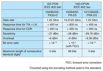
Below, we discuss the international standard specifications and characteristics of burst-mode receivers. 3. International standard specificationsThe specifications for 10-Gbit/s PON-system (10G-EPON (10-Gbit/s Ethernet PON), IEEE 802.3av) [3] burst-mode receivers, as defined by IEEE, are shown in Table 1. For comparison, the table also shows the specifications for the 1-Gbit/s PON system (GE-PON (Gigabit Ethernet PON), IEEE 802.3ah) [4] currently in common use. For the 10G-EPON system, both 10- and 1-Gbit/s burst signal rates are stipulated. For signals at each rate, burst-mode receivers must satisfy the values in the table for optical input sensitivity and overload (tolerance to strong signals) just like continuous-mode receivers. Characteristics particular to burst-mode receivers are the response times. For 10-Gbit/s receivers, the response times of the TIA and LA are twice those in 1-Gbit/s receivers, and the time allowed for the CDR to extract signal timing has not changed. However, the maximum number of consecutive identical digits (CIDs) (zero or one) has been increased to 66 bits. This means that when a signal begins suddenly after a period of no signal, the TIA and LA must adjust the amplification, and the CDR must match the signal timing within a short time (although it is 1.5 times the previous time). On the other hand, each integrated circuit (IC) must not change state within a CID period (the same as when there is no signal) that is over 13 times longer than that specified for 1 Gbit/s. These requirements appear to conflict: they require a fast response while also requiring that the state does not change.
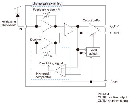
4. Burst-mode receiver circuitsBelow, we introduce receiver circuits that satisfy the particular requirements of burst signals. 4.1 Burst-mode transimpedance amplifier (B-TIA)A block diagram of a B-TIA [5] is shown in Fig. 3. In order to respond to a sudden input signal and instantly set the gain optimally, the circuit switches between two feedback resistor values Rf. When the input signal is weak, a high feedback resistance is used for high gain, and when the input signal strength exceeds a set value, the TIA switches to a low feedback resistance for lower gain. Existing circuits either do not switch feedback resistance or vary it continuously. In the former case, when the sensitivity is set to handle weak signals, strong signals produce signal distortion, while when it is set to handle strong signals, the sensitivity is not enough for weak signals. In the latter case, when the response time controlling the feedback resistance is fast, sensitivity changes during a CID period. If the response is made slower to prevent this, the burst response is somewhat slower, which is a drawback. Switching between two values allows for a fast response, and a comparator that has hysteresis is used to preserve the post-switching state, which enables good CID reception.
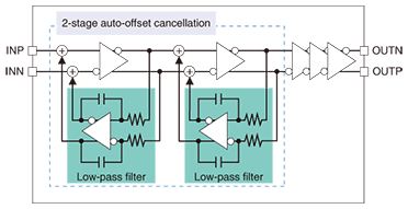
4.2 Burst-mode limiting amplifier (B-LA)A block diagram of a B-LA [6] is shown in Fig. 4. The basic function of the LA is to receive an input voltage signal with a varying amplitude (ranging from small to large) and to output a fixed-amplitude signal. For burst signals, another function is also important: the B-LA adjusts the voltage levels of positive and negative signals quickly (see Fig. 2), which is called offset cancellation. When a burst signal arrives after a period of no signal, the positive input (INP) of the LA goes to high with respect to a fixed center level and the negative input (INN) goes to low. The LA output signal first appears when the positive and negative signals cross, so to reduce the amount of time until a signal is output, a means of ensuring fast offset cancellation is needed. In the first offset cancellation stage in Fig. 4, the average level of the negative output of the first stage is fed back to the positive input and vice versa. This causes both signals to approach the same potential. We get a second-order filter effect by connecting two such circuits in series. With a second-order filter, the first state change is slow and the subsequent change is fast. Therefore, while reducing the level variation due to CID, the second-order filter can cancel the offset quickly for both positive and negative signals at the beginning of a burst and can reduce the time until the burst signal is output.
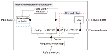
4.3 Burst-mode clock and data recovery (B-CDR)A block diagram of a B-CDR circuit [7] is shown in Fig. 5. This CDR is based on a gated voltage-controlled oscillator (GVCO) that has the fastest synchronization time to the input signal. When the input signal rises from low to high, a pulse is output from the gating circuit. When this pulse is input to a NAND gate, which is one of the ring gates in GVCO1, the clock timing of GVCO1 adjusts to the data in that single pulse. Since the matching of the timing is so fast, any jitter in the input signal appears as-is in the output clock of GVCO1, so synchronization loss problems may occur in later-stage circuits. Moreover, when the high width of an input signal is much shorter than the low width, the decision circuit (DEC) produces a false detection. For this design, a second oscillator (GVCO2) is placed in series with the first. By inputting the output clock from GVCO1 attenuated in the buffer (Buf), we were able to obtain a stable output clock that was less affected by the jitter in the input signal. Moreover, by adding a feedback loop that monitors the input signal pulse width and compensates for its distortion, we were able to make the pulse widths for high and low symbols close to one another.
5. Burst-mode receiver characteristicsMicrographs of IC prototypes of the B-TIA, B-LA, and B-CDR for the burst-mode receiver are shown in Fig. 6. We selected a silicon process to fabricate these ICs, putting priority on high-volume production and low cost considering that they are for access network services. Taking into consideration their high-frequency characteristics, we housed each IC in a package for high-speed IC applications, mounted each package on an evaluation board, and evaluated their characteristics as a burst-mode receiver.
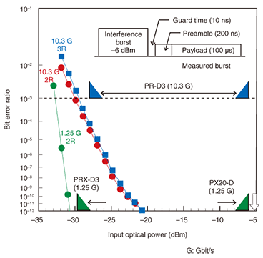
The evaluation results are shown in Fig. 7. We varied the power of the input optical burst signal and measured the bit error ratio (BER) in the output signal payload. To ensure that measurements reflected the receiver’s longest (worst-case) possible response time, we input a signal of the maximum strength indicated in the specifications directly before inputting a signal of the strength being measured. Points labeled 2R are the BERs for the TIA + LA output, while 3R is the BER that also includes the CDR. For both 10 Gbit/s and 1 Gbit/s, the receive sensitivity and overload values met those in the standards specifications shown in Table 1. The receiver can set the gain and adjust the timing within a preamble time of 200 ns. This indicates that the receiver achieves a very fast burst-response time of less than one sixth of the 1200 ns specified in the 10G-EPON standard.
6. Future developmentsIn the future, we plan to use this technology in our research and development of higher-layer LSIs to promote the use of 10G-EPON in Japan and around the world and to develop circuit techniques with even better energy-saving characteristics, as this becomes more and more important. References
|
||||||||||||||||||||||||||