|
|||||||||||||||||||||||||||||||||||||||||||||||||||||||||||||||
|
|
|||||||||||||||||||||||||||||||||||||||||||||||||||||||||||||||
       |
Feature Articles: R&D of Optical Component Technologies for 100-Gbit/s Digital Coherent Communications Vol. 9, No. 3, pp. 48–54, Mar. 2011. https://doi.org/10.53829/ntr201103fa8 Multilevel Optical Modulator Utilizing PLC-LiNbO3 Hybrid-integration TechnologyAbstractMultilevel optical modulators are key devices for optical transmission systems with transmission rates of 100 Gbit/s and beyond. For such modulators, NTT Photonics Laboratories has developed hybrid-integration technology for silica planar lightwave circuits (PLCs) and LiNbO3 phase modulator arrays. This makes possible various kinds of multilevel modulator featuring a compact size, low loss, and high scalability. We review our recent progress in PLC-LiNbO3 technology and describe some integrated multilevel modulators: 100-Gbit/s PDM-QPSK and post-100G OFDM-QPSK and 64QAM modulators (PDM: polarization-division multiplexing, QPSK: quadrature phase-shift keying, 100G: 100-Gbit/s, OFDM: orthogonal frequency-division multiplexing, QAM: quadrature amplitude modulation). 
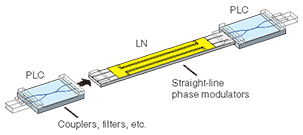
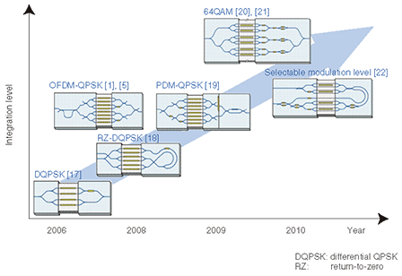
1. IntroductionFuture large-capacity wavelength-division-multiplexing (WDM) transmission systems will require advanced spectrally efficient multilevel modulation formats, such as N-level phase-shift keying (N-PSK), N-level quadrature amplitude modulation (N-QAM), and orthogonal frequency-division multiplexing (OFDM), combined with polarization-division multiplexing (PDM) [1]. High-level QAMs have been used in the latest record-setting experiments: transmission of 69.1 Tbit/s using PDM-16QAM [2], the highest spectral efficiency (SE) for 100-Gbit/s/ch-class transmission of 9.0 bit/s/Hz with PDM-64QAM [3], and the highest potential SE of 12.4 bit/s/Hz with PDM-512QAM [4] (ch: channel). OFDM is promising not only for achieving a high SE [5], but also for enabling a bandwidth-variable optical network for efficient use of the spectral resource [6]. To accomplish those advanced modulations, multilevel electronics, such as arbitrary waveform generators or digital-to-analog converters, have been used in many transmission experiments [3], [4], [7]. They let us cover various modulation formats with a simple optical setup. On the other hand, optical multilevel-signal syntheses, in which only binary electronics are used, have also been studied extensively [2], [5], [8]–[22]. Those schemes are promising for high-speed multilevel modulations because binary electronics pose fewer challenges for high-speed operation than multilevel electronics do [13], [15], [16]. In this article, we briefly review technologies for optical multilevel-signal syntheses and describe our recent work on integrated multilevel optical modulators using a hybrid configuration of silica planar lightwave circuits (PLCs) and LiNbO3 (LN) phase modulators. 2. Optical multilevel-signal syntheses and integrated optical modulatorsThere have been many studies in which multilevel optical modulations are achieved with combinations of simple commercially available modulators, such as Mach-Zehnder modulators (MZMs), straight phase modulators, and I/Q modulators with a dual-parallel MZM configuration (I: in-phase component, Q: quadrature component). By connecting those modulators in tandem and adjusting the amplitude of each binary driving signal to an appropriate value, researchers have achieved multilevel modulations, such as 8PSK [8], 16APSK [9], [10], 8QAM [11], and 16QAM [11], with high baud rates (ASPK: amplitude and phase key shifting). Integrated multilevel modulators have also attracted much attention [12]–[22]. The integration provides two major advantages. First, the transmitter setup is significantly smaller. Second, we can connect modulator components in parallel much more easily than in the case of discrete modulators because integration eliminates fiber connection, which causes optical-phase fluctuation. A parallel configuration enables us to use superposed modulation, which was originally demonstrated with high-speed microwave transmission [23]. Integrated modulators for 16QAM have been demonstrated with several configurations, such as a quad-parallel MZM configuration fabricated with LN and PLCs [12], a five-arm configuration with quad-parallel electro-absorption modulators fabricated with InP [13], and a dual-parallel dual-tandem MZM configuration fabricated with LN [14]. In multilevel modulator design, it is worth exploiting a particular characteristic of MZMs. When the MZM is driven in a push-pull condition with a signal amplitude of 2Vπ (binary PSK mode), the output optical signal has smaller distortions in symbol levels than the driving electrical signal. This is because the output optical field of the MZM varies sinusoidally with the driving voltage [15]. For various modulation formats, transmitter configurations with only 2Vπ MZMs have also been investigated [15], [16]. The key to implementing those all-2Vπ-MZM configurations is the integration of MZMs and high-quality passive optics because accurate control of the relative optical amplitude and phase in each optical path is required. To achieve such integrations with high performance levels, we have been developing hybrid integration technology for PLCs and LN phase modulators. 3. PLC-LN modulators3.1 Basic structure and conceptThe basic structure of a hybrid-integrated PLC-LN modulator is shown in Fig. 1. We use an LN chip containing an array of simple straight phase modulators and PLCs containing all the other circuit components, such as couplers and filters. This structure combines the large electro-optic bandwidth of LN and the excellent transparency and design flexibility of PLCs. Another advantage is that this configuration is highly scalable because we can increase the integration level by increasing the number of phase modulator arrays in the LN chip and devising PLCs with corresponding complexity. As shown in Fig. 2, we have developed various modulators with increasing integration levels [17]–[22]. Each modulator circuit consists only of 2Vπ MZMs and passive components. Below, we describe PLC-LN modulators based on PDM-QPSK for 100 Gbit/s and based on OFDM-QPSK and 64QAM for post-100G applications. We also briefly describe a modulator with a selectable modulation level for post-100G applications.
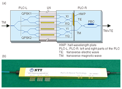
3.2 100-Gbit/s PDM-QPSK modulatorThe configuration of the PDM-QPSK modulator [19] utilizing PLC-LN integration technology is shown in Fig. 3(a). Eight straight phase modulators with four high-speed signal electrodes in a Z-cut LN chip and thirteen couplers in PLCs make up two QPSK modulator circuits connected in parallel. In addition, a polarization multiplexing circuit, consisting of a polarization rotator with a half-wavelength plate, and a waveguide polarization beam combiner (PBC) are connected to their output. A PLC-type PBC is a compact Mach-Zehnder interferometer (MZI) about 10 mm in length and has an excellent polarization extinction ratio of greater than 25 dB over the whole C-band wavelength range [24]. A photograph of this module is shown in Fig. 3(b). The module package size is 118 mm × 13.5 mm × 7 mm. Including the fiber boots on both sides, it is 131 mm long, which approaches the smallest size ever reported.
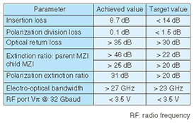
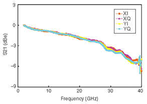
Typical characteristics of a 100-Gbit/s PDM-QPSK modulator are listed in Table 1. The overall optical insertion loss of our PDM-QPSK modulator is 8.7 dB at a wavelength of 1.55 μm including a polarization division intrinsic loss of 3 dB. The modulator’s frequency response is shown in Fig. 4. XI, XQ, YI, and YQ correspond to the four MZMs shown in Fig. 3(a).
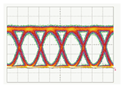
The modulator has an electro-optic 3-dB bandwidth of more than 27 GHz. The driving voltage was less than 3.5 V at 32 Gbit/s. The measured eye pattern for a driving voltage of 3.0 V when the modulator was driven with 32-Gbit/s non-return-to-zero 231-1 pseudorandom bit sequences in a back-to-back setup is shown in Fig. 5. Clear eye opening was obtained in this experiment. The Optical Internetworking Forum (OIF) standardized a 100-Gbit/s integrated modulator in April 2010 [25]. Our 100-Gbit/s PDM-QPSK modulator complies with the target specifications.
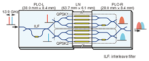
3.3 OFDM-QPSK modulatorThe configuration of the OFDM-QPSK modulator [1], [5] is shown in Fig. 6. The modulator integrates a PLC interleave filter, two QPSK modulation circuits, each with a dual-parallel MZM configuration, and an output coupler. The input light for this modulator consists of two subcarriers, which can be generated by using another MZM driven with a clock signal. The subcarriers are separated by the interleave filter and modulated by different QPSK modulation circuits. The two QPSK signals are finally coupled and the modulator outputs a two-subcarrier OFDM-QPSK signal. The baud rate of the modulation, which is equal to the frequency spacing between the subcarriers, is 13.9 Gbaud.
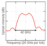
The spectrum of a 111-Gbit/s PDM-OFDM-QPSK signal generated with the modulator and an external PDM circuit is shown in Fig. 7. The signal bandwidth is 42 GHz, which is 1.5 times the baud rate and narrow enough for 50-GHz-grid WDM transmission. Using this modulator, we achieved 13.5-Tbit/s (135 × 111-Gbit/s/ch) WDM transmission over a distance of 7209 km [1], [5].
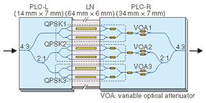
3.4 64QAM modulatorThe configuration of the 64QAM modulator [20], [21] is shown in Fig. 8. Three QPSK modulation circuits, each consisting of dual-parallel MZMs, are connected in parallel by a pair of PLC asymmetric 1×3/3×1 splitter/combiners, each with a power splitting/combining ratio of 4:2:1. These asymmetric circuits were designed using the wavefront-matching method, which lets us optimize the waveguide pattern on the basis of the desired splitting/combining ratio. PLC variable optical attenuators enable fine tuning of the power ratio. The 64QAM signal is synthesized by coupling the three QPSK signals with a field-amplitude ratio of 4:2:1 (power ratio of 16:4:1). The module has a small overall optical insertion loss of 5.5 dB, as well as a broad electro-optic bandwidth of >25 GHz.
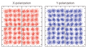
By driving the modulator with six 20-Gbaud binary data signals and using an external PDM circuit, we generated a 240-Gbit/s PDM-64QAM signal [20]. The signal was received with a coherent receiver using a pilotless demodulation algorithm in an offline digital signal processor. The constellations obtained with a back-to-back intradyne setup are shown in Fig. 9. The 64 signal points are clearly distinguished. The bit-error rate was better than 1.3 × 10⁻². Thus, we successfully demonstrated the record bit rate of 240 Gbit/s for PDM-64QAM using the modulator.
3.5 Selectable-modulation-level modulatorWe also developed a selectable-modulation-level modulator that lets us select QPSK, 8PSK, 8QAM, or 16QAM [22], [26]. This modulator was devised for use in optical networks with a flexible modulation format, which have become the focus of attention in recent years [6]. In this modulator, we can flexibly and adaptively select a suitable multilevel modulation scheme taking account of the transmission condition. 4. ConclusionWe have developed PLC-LN hybrid integration technology for advanced multilevel modulators. Utilizing this technology, we have demonstrated various advanced multilevel modulators, such as a PDM-QPSK modulator for 100 Gbit/s and an OFDM-QPSK modulator, a 64QAM modulator, and a selectable-modulation-level modulator for post-100G applications. Each modulator shows excellent characteristics in terms of compact size and low insertion optical loss and a practical level of optical loss and electro-optic bandwidth. This technology is promising for optical transmission systems with channel rates of 100 Gbit/s/ch and beyond and a transfer rate well above 10 Tbit/s and for future optical networks. AcknowledgmentsThis work is partly supported by the R&D projects on “High-speed Optical Transport System Technologies” and “High-speed Optical Edge Node Technologies” of the Ministry of Internal Affairs and Communications (MIC) of Japan. References
|
||||||||||||||||||||||||||||||||||||||||||||||||||||||||||||||