 |
|||||||||||||||||||||||||||||||||
|
|
|||||||||||||||||||||||||||||||||
       |
Feature Articles: R&D of Optical Component Technologies for 100-Gbit/s Digital Coherent Communications Vol. 9, No. 3, pp. 55–61, Mar. 2011. https://doi.org/10.53829/ntr201103fa9 100-Gbit/s Optical Receiver
|
||||||||||||||||||||||||||||||||

| † | NTT Photonics Laboratories Atsugi-shi, 243-0198 Japan |
|---|
1. Configuration of digital coherent receiver
Digital coherent communication technology, which is based on techniques for multilevel phase modulation and digital coherent reception, is being studied as a way to achieve ultrahigh-speed photonic networks with a bit rate of 100 Gbit/s or more per channel. Among several reported modulation formats and multiplexing techniques, polarization division multiplexed quadrature phase shift keying (PDM-QPSK)*1 is promising for spectral efficiency and resistance to various types of dispersion, and it is being developed intenisively.
The basic configuration of the PDM-QPSK digital coherent receiver is shown in Fig. 1 [1]. The receiver is composed of an optical front-end (FE), which includes components from the optical input section to the transimpedance amplifiers (TIAs), analog-to-digital converters (ADCs), and a digital signal processor (DSP).
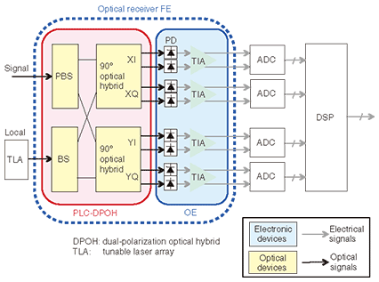
Fig. 1. Configuration of digital coherent receiver.
The optical receiver FE consists of an optical signal processing section with a polarization beam splitter (PBS), a beam splitter (BS), and two 90° optical hybrid mixers and an optical-to-electrical (OE) conversion section with eight photodiodes (PDs) and four TIAs. With this receiver FE, the input PDM-QPSK-modulated signal light is separated into orthogonal polarization components (X/Y polarized waves) and orthogonal phase components (I/Q channels; I: in-phase component, Q: quadrature component), which are converted into four high-speed differential electrical signals and output.
The optical receiver FE has functions for optical-domain signal processing and OE conversion and is composed of many optical/electrical components. This creates a need for high-density and well-controlled fabrication techniques for optoelectronic integration.
| *1 | PDM-QPSK: A type of phase modulation for digital signals. Two bits of data are allocated using four phase modulations on each of the TE- and TM-polarized lights. |
2. Fabrication issues and approaches for optical receiver FE
Compared with conventional intensity modulation direct detection methods, the digital coherent optical receiver FE requires more-sophisticated functionality. This is because precise and stable optical signal processing is required to separate the X/Y and I/Q components, and the phase and amplitude of the separated signals must be preserved in the connection from the optical stage to the electrical stage in order to achieve the required receiver performance. However, in conventional technologies using multiple optical fibers interconnecting individual devices, it is difficult to consistently control the optical phase and differential delay between fibers. In other words, implementation of the signal processing from the optical stage through to the electrical stage in a stable integrated circuit has been a critical issue for achieving a practical, digital coherent optical receiver FE and obtaining the required receiver performance.
At NTT Photonics Laboratories, we are developing basic techniques for hybrid integration using silica-based planar lightwave circuits (PLCs). We have successfully fabricated an integrated optical receiver FE module incorporating all the required functions, including a PBS, in a single package [2].
3. Module structure of integrated optical receiver FE and developed techniques
A photograph of the integrated optical receiver FE module with the upper cover removed is shown in Fig. 2. The FE is composed of optical signal processing circuits and the OE sub-assembly. We integrated the optical signal processing section including PBS, BS, and two 90° optical hybrid mixers in a single-chip PLC. The OE sub-assembly contains PD and TIA arrays in a compact, hermetically sealed package. A cross-section of the structure near the optical connection between the PLC and OE subassembly is illustrated in Fig. 3. The multiport optical connection between the PLC output ends and the PD array mounted in the OE subassembly is implemented with a micro optic system using a micro-lens array and 90° folding mirror. The power supply and electrical control and signal-output lines are all connected to an external board by flexible printed circuit boards. The module size is 27 × 50 × 6 mm3. The hybrid integration structure lets us use appropriate devices with optimal materials and structures for both the optical signal processing and OE conversion sections, enabling us to achieve compact integration while maintaining maximal performance and reliability for the module as a whole.
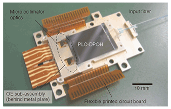
Fig. 2. Integrated optical receiver front-end module.
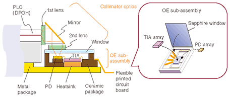
Fig. 3. Integration structure.
Below, we give an overview of the elemental technologies developed for this integration.
3.1 Digital coherent optical receiver circuit integrated on a single silica PLC chip
The optical signal processing required on the optical receiver FE needs stable and highly accurate control of optical phase and interference. To achieve this, we designed a single-chip PLC integrating two PBSs and two 90° optical hybrids [3]. We call this circuit a dual-polarization optical hybrid (DPOH). The circuit configuration is shown in Fig. 4. The PBS consists of a Mach-Zehnder interferometer*2 with grooves formed near one waveguide arm, giving a phase difference of π to the orthogonal polarized waves [4]. This configuration yields a PBS that outputs TE-polarized light from the cross port and TM-polarized light from the through port (TE: transverse electric, TM: transverse magnetic).
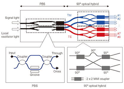
Fig. 4. Circuit configuration of dual polarization optical hybrid (DPOH).
The 90° hybrid is structured with optical waveguides arranged to interlace with optical couplers, and 2 × 2 multi-mode interference (MMI) couplers are used. There are various kinds of waveguide-type optical hybrids, such as a slab coupler [5] and a 4 × 4 MMI coupler [6], but this circuit with the interlaced optical-coupler has the benefits of achieving both low loss and orthogonality (phase difference of 90°).
For the DPOH, important performance indexes are the polarization extinction ratio in the PBS, orthogonality in the optical hybrid, and losses and deviations. The fabricated DPOH exhibited excellent results for these: we measured excess loss of less than 2.5 dB, loss deviations of less than 0.2 dB, and a polarization extinction ratio greater than 25 dB. As shown in Fig. 5, good values for orthogonality were also obtained: less than ±1° over the wide wavelength range from 1520 nm to 1620 nm.
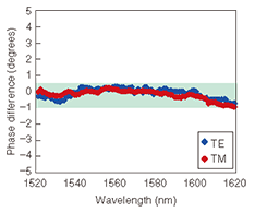
Fig. 5. Phase difference of fabricated DPOH.
3.2 Compact, hermetically sealed OE subassembly
The optical-receiver-FE’s OE-conversion section requires high reliability and high-speed operation for receiving 100-Gbit/s-class PDM-QPSK signals. Moreover, for hybrid integration, an optical interface for multi-port optical connection to the optical waveguides is required. We have developed a compact, hermetically sealed OE sub-assembly that meets these requirements.
The OE sub-assembly consists of a layered alumina-ceramic cavity in which the two-channel dual-PD and two-channel TIA arrays are assembled (Fig. 3). The high-frequency signal lines and power/control electrical wiring are also formed on the ceramic layer. The upper surface of the cavity is hermetically sealed by a sapphire window and AuSn solder. The size of the fabricated OE subassembly is 8.2 × 9.2 × 1.4 mm3. We confirmed that the high-frequency signal lines on this package have a 3-dB transmission bandwidth of more than 40 GHz. The sapphire window provides the hermetic seal required to ensure reliability of the InP semiconductor device while also functioning as the optical interface: it provides an optical window and a fixed surface for the optical connection to external devices. This structure allows us to obtain efficient multi-port optical connections between incident lights and the PD array by using a micro-lens array.
3.3 Multi-port optical connection using micro-lens array
The optical connection between the DPOH and PD must be small in size and have low losses and stability with respect to fluctuations in ambient temperature. To achieve this, we chose to use a micro collimated optical system using a micro-lens array. The first lens is at the PLC’s output facet and the second lens is on the surface of the sapphire window of the OE sub-assembly; these lenses were fixed with ultraviolet-curable adhesive. We used a mirror between the two lenses to change the optical axis of the light emitted from the PLC by 90° and inject it into the PD. With this structure, we achieved an extremely compact optical connection with an optical path length of only about 2.5 mm.
In designing the optical system, it is important to ensure a wide tolerance so as to avoid PD responsivity degradation and port-to-port deviation, even when the positions of the PLC output ends and PDs shift owing to ambient temperature variation. For the fabricated receiver FE module, the maximum optical misalignment caused by differences in thermal expansion coefficients across the operating temperature range of -5 to 80°C was estimated to be ±5 μm, so the module was designed to handle this. The measured tolerance of the designed micro collimator optics system was more than ±10 μm for a 0.2-dB-down width, ensuring sufficient tolerance for the operating temperature range.
| *2 | Mach–Zehnder interferometer: An optical circuit configuration that uses interference between two optical paths to change the light intensity. |
4. Characteristics of fabricated PDM-QPSK coherent receiver FE module
The measured responsivity for all ports on the fabricated receiver FE module is shown in Fig. 6. It includes the sensitivity characteristics of the PDs themselves as well as an intrinsic loss of 9 dB from the DPOH. Besides these, excess losses caused by the optical system were estimated to be 0.4 dB, and the responsivity deviation between adjacent PDs was less than 0.4 dB, so we achieved good optical connection performance in terms of both losses and deviation. The relationship between ambient temperature and responsivity is shown in Fig. 7. The responsivity variation was less than ±0.25 dB in the operating temperature range of -5 to 80°C.
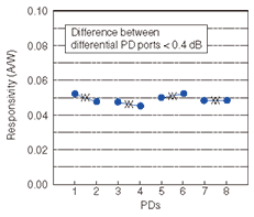
Fig. 6. Responsivity of fabricated optical receiver FE module.
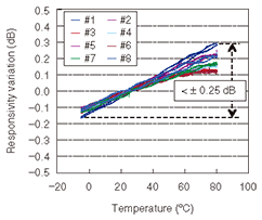
Fig. 7. Relationship between responsivity and temperature.
Next, we tested the receiver operation for a 112-Gbit/s PDM-QPSK signal. The constellation plot and relationship between optical signal-to-noise ratio (OSNR) and Q-factor are shown in Fig. 8. These results confirm stable operation as a 100-Gbit/s-class optical receiver FE.
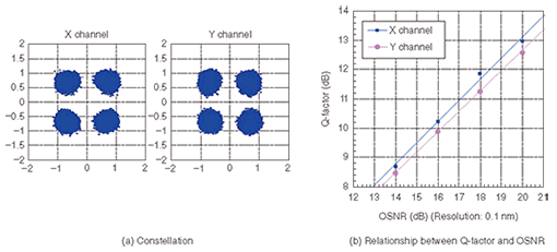
Fig. 8. Receiver characteristics for 112-Gbit/s PDM-QPSK signal.
5. Future plans
We plan to make further improvements to the key device technology such as PLC, PD, and TIA, and their integration technology. We will also expand their applications in next-generation optical integration modules needed for 100-Gbit/s-class-and-higher multilevel-modulation optical transmission systems.
Acknowledgments
This work is partly supported by the R&D projects on “High-speed Optical Transport System Technologies” and “High-speed Optical Edge Node Technologies” of the Ministry of Internal Affairs and Communications (MIC) of Japan.
References
| [1] | http://www.oiforum.com/public/documents/OIF_DPC_RX-01.0.pdf |
|---|---|
| [2] | T. Ohyama, I. Ogawa, H. Tanobe, R. Kasahara, S. Tsunashima, T. Yoshimatsu, H. Fukuyama, T. Itoh, Y. Sakamaki, Y. Muramoto, H. Kawakami, M. Ishikawa, S. Mino, and K. Murata, “All-in-one 100-Gbit/s DP-QPSK Coherent Receiver Using Novel PLC-based Integration Structure with Low-loss and Wide-tolerance Multi-channel Optical Coupling,” Proc. of OECC 2010, PD6, Sapporo, Japan. |
| [3] | Y. Sakamaki, H. Yamazaki, T. Mizuno, T. Goh, Y. Nasu, T. Hashimoto, S. Kamei, K. Hattori, H. Takahashi, T. Kobayashi, and M. Ishikawa, “Dual polarisation optical hybrid using silica-based planar lightwave circuit technology for digital coherent receiver,” Electron. Lett., Vol. 46, No. 1, pp. 58–60, 2010. |
| [4] | Y. Hashizume, R. Kasahara, T. Saida, Y. Inoue, and M. Okano, “Integrated Polarisation Beam Splitter Using Waveguide Birefringence Dependence on Waveguide Core Width,” Electron. Lett., Vol. 37, No. 25, pp. 1517–1518, 2001. |
| [5] | C. R. Doerr, D. M. Gill, A. H. Gnauck, L. L. Buhl, P. J. Winzer, M. A. Cappuzzo, A. Wong-Foy, E. Y. Chen, and L. T. Gomez, “Monolithic Demodulator for 40-Gb/s DQPSK Using a Star Coupler,” J. of Lightwave Technol., Vol. 24, No. 1, pp. 171–174, 2006. |
| [6] | H. -G. Bach, A. Matiss, C. C. Leonhardt, R. Kunkel, D. Schmidt, M. Schell, and A. Umbach, “Monolithic 90° Hybrid with Balanced PIN Photodiodes for 100 Gbit/s PM-QPSK Receiver Applications,” Proc. of OFC2009, OMK5, San Diego, CA, USA. |
 |
|
|---|---|
 |
|
 |
|
 |
|
 |
|
 |
|
 |
|