|
|||||||||||||||||||||||||||||||||
|
|
|||||||||||||||||||||||||||||||||
       |
Regular Articles Vol. 9, No. 4, pp. 36–43, Apr. 2011. https://doi.org/10.53829/ntr201104ra1 High-speed Low-power Digital-to-Analog Converter Using InP Heterojunction Bipolar Transistor Technology for Next-generation Optical Transmission SystemsAbstractWe have developed a high-speed low-power 6-bit digital-to-analog converter (DAC) for next-generation optical transmission systems. To achieve both high-speed and low-power performance, we used a simple R-2R ladder-based current-steering architecture and devised a new timing alignment technique. A DAC test chip was fabricated using our in-house InP-based heterojunction bipolar transistor (HBT) technology. It operates at a sampling rate of up to 28 giga-samples per second (GS/s) with low-power consumption of 0.95 W and achieves a better figure of merit (0.53 pJ per conversion step) than any other previously reported DAC with a sampling rate above 20 GS/s. It also provides a clear multilevel modulated signal and can be applied to post-100-Gbit/s/ch multilevel optical transmission systems. 
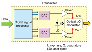
1. IntroductionCoherent optical data transmission schemes with multilevel modulation formats are now attracting a great deal of attention and are being investigated in terms of suitability for future cost-effective optical transport networks. High-order multilevel modulation formats, such as 16-QAM and 64-QAM (QAM: quadrature amplitude modulation), are especially promising techniques for constructing post-100-Gbit/s/ch optical transmission systems [1]–[3]. An example of a transmitter for such systems is shown in Fig. 1. In the transmitter, high-speed digital-to-analog converters (DACs) are key components for generating modulated signals. DAC performance requirements depend on the target bit rate and the modulation format. For example, for a 160-Gbit/s/ch-class polarization-division-multiplexing (PDM) 16-QAM system, which has a baud rate of 20 Gbaud, a sampling rate of above 20 giga-samples per second (GS/s) and a resolution of 6 bits or more are needed.
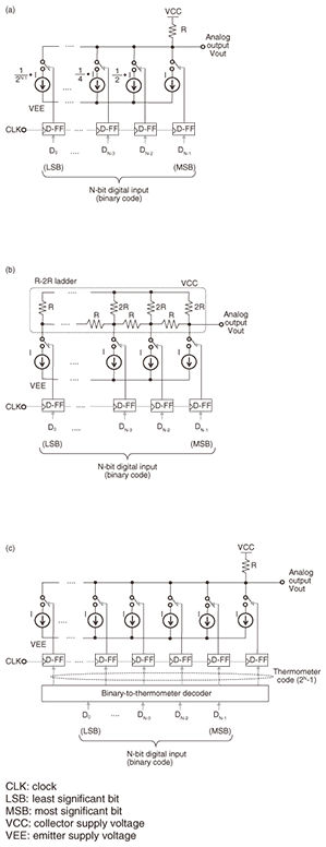
Recently, high-speed (> 20 GS/s) 6-bit DACs based on SiGe heterojunction bipolar transistor (HBT) technology for such optical transmission systems have been reported [4]–[6]. Recent scaled SiGe HBT technology offers high-speed operation, but care is often needed to avoid device mismatch, such as transistor variation, especially for mixed-signal integrated circuits (ICs), such as DACs. They achieve a sampling rate of over 20 GS/s, but consume more than 2 W owing to their complicated circuit architectures to overcome device mismatch and improve their linearity. This article describes the circuit design and measured performance of a high-speed low-power DAC using InP HBT technology. InP HBT technology offers high-speed operation with larger devices than SiGe HBT technology because of its inherent excellent high-speed performance. Therefore, it provides higher tolerance to device mismatch and a higher breakdown voltage with the drawback of smaller-scale integration. It enables us to choose a simpler circuit architecture and helps achieve low-power operation. InP HBTs are attractive for making high-speed, low-power, high-sensitivity mixed-signal ICs, such as DACs. We previously reported a 32-GS/s 6-bit 1.4-W DAC [7] using our in-house 1-μm-emitter InP HBT technology, which yields a peak cutoff frequency (ft) of 175 GHz and a peak maximum oscillation frequency (fmax) of 260 GHz. In this article, we present our updated lower-power DAC using the same technology [8]. To achieve high speed, lower power, and higher dynamic linearity, we used a simple R-2R ladder-based current-steering architecture and devised a new timing alignment technique, which helps suppress the glitch noise in the analog output and achieve high dynamic linearity. The DAC with the timing alignment technique can operate at a sampling rate of up to 28 GS/s and has, at the same time, high dynamic linearity with low-power consumption of 0.95 W. It also provides a clear multilevel modulated signal and can be applied to post-100-Gbit/s/ch optical transmission systems. This article is organized as follows. Section 2 describes the circuit design of the high-speed low-power DAC. Section 3 presents measurement results for the test chip. Section 4 compares our DAC with state-of-the-art DACs. Finally, section 5 summarizes this work. 2. Circuit design2.1 Current-steering DACsMost high-speed DACs are based on a current-steering architecture [9], [10]. There are three main ones for high-speed DACs, as shown in Fig. 2: binary-weighted current-steering DAC, R-2R ladder-based current-steering DAC, and segmented current-steering DAC.
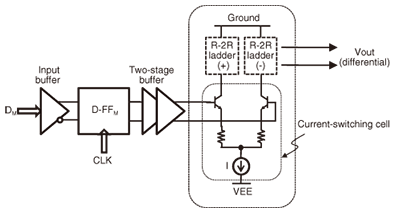
The binary-weighted current-steering DAC consists of binary-weighted current sources, current switches, a single resistor (R), and D-type flip-flops (D-FFs). The D-FFs are placed just before current switches to reduce the timing skew of incoming digital data (D0–DN-1). This DAC has the simplest architecture but the highest demand for the matching requirement. It is hard to implement accurate binary-weighted current sources for high-resolution DACs. The R-2R ladder-based current-steering DAC is one solution for achieving higher resolution. In this architecture, each current source has the same value. The R-2R ladder network can be implemented with a combination of unit resistors. Therefore, it is easier to achieve relative matching among devices and implement higher resolution. The segmented current-steering DAC has a binary-to-thermometer-code decoder and 2N-1 identical current sources. This architecture has the highest tolerance to device mismatch, but needs additional building blocks and many parallel current switches and consumes much more power than the other two. A simpler architecture is a better choice for achieving both high-speed and low-power operation. However, one should choose an architecture by considering the strengths and weaknesses of the given technology. For example, high-speed 6-bit DACs with scaled SiGe HBT technology are based on a partially segmented architecture, which is a combination of segmented and binary-weighted architectures, to overcome device mismatch and achieve high linearity. On the other hand, our in-house InP HBT technology enables us to choose a simpler R-2R ladder-based architecture for 6-bit resolution. Therefore, an R-2R ladder-based current-steering architecture is an appropriate choice for our InP HBT technology to achieve a DAC that features both high speed and low power. However, with an R-2R ladder-based current-steering DAC, one must pay careful attention to glitch noise in the analog output, which is caused mainly by the timing skew of the digital data that controls the current switches. As the sampling rate increases, it becomes more difficult to distribute the clock signal simultaneously among the retiming D-FFs. In other words, when the sampling rate is very high, the D-FFs cannot suppress the timing skew of the incoming data, resulting in large glitches in the analog output, especially when the data changes from “011111” to “100000” where all current switches change. Thus, this DAC requires very strict timing alignment. In our previous work [7], to overcome this problem we devised a novel double-sampling technique that relaxes the speed restraint on the clock distribution. However, it needs additional circuits and therefore consumes additional power. In this work, to achieve high speed, lower power, and higher dynamic linearity, we devised a new timing alignment technique that helps achieve accurate timing alignment for the current switches and suppress the glitch noise in the analog output without any additional circuits, as explained in section 2.2. 2.2 Timing alignment techniqueA simplified schematic of the R-2R ladder-based current-steering DAC used in this work is shown in Fig. 3. The building blocks have a differential architecture (Fig. 4). The incoming data (DM) is converted into a differential signal in the input buffer. This differential signal is then latched and retimed by the D-FF on the basis of a standard master-slave flip-flop. There is a two-stage buffer between the D-FF and current switch to eliminate clock noise and suppress the data feed-through. The retimed and smoothed differential signal drives the current switch, which is based on a differential pair with emitter-degeneration resistors to suppress the overshoot in the analog output. We carefully designed the differential R-2R ladders to have an output impedance of 50 Ω to match the 50-Ω load.
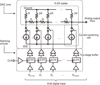
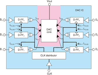
As mentioned in section 2.1, we devised a timing alignment technique to help achieve accurate timing alignment for the current switches. This technique is based on the layout and wiring techniques. The rough layout of the 6-bit DAC test chip is shown in Fig. 5. The DAC core consisting of six current-switching cells and differential R-2R ladders was placed at the center of the chip. Six retiming D-FFs were symmetrically placed around the DAC core. The clock paths from the clock distributor to the upper four D-FFs (LCLK5–LCLK2) were designed to be equal in length. The data paths from the upper four D-FFs with the two-stage buffers to the upper four current switches (LD5-LD2) were also designed to be equal in length. Therefore, the clock and data paths for the upper four bits are fully symmetrical. On the other hand, the clock paths from the clock distributor to the lower two D-FFs (LCLK1 and LCLK0) were designed to be equal in length but shorter than the upper four. The difference in length between the upper four and the lower two causes timing skew between the upper four data and the lower two data. To suppress this timing skew, the paths from the lower two D-FFs with the two-stage buffers to the lower two current switches (LD1 and LD0) were designed to be longer than the upper four. In short, we designed the interconnect paths to satisfy the following equation: 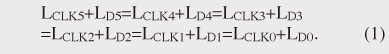
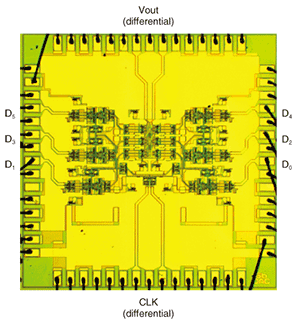
With these layout and wiring techniques, all 6-bit data (D0–D5) can be aligned accurately at the current switches. The DAC consequently has small glitches and achieves good dynamic linearity without additional circuits. 3. Measured results3.1 Process technologyThe 6-bit DAC test chip was fabricated using our in-house InP HBT technology [11]. Each HBT has a 70-nm-thick undoped InP emitter, a 50-nm-thick carbon-doped InGaAs base, and a 300-nm-thick InGaAs collector. The size of the lateral emitter of the standard HBT is 1 μm × 4 μm. The fabricated HBTs have a peak cutoff frequency (ft) of 175 GHz and a peak maximum oscillation frequency (fmax) of 260 GHz. The technology also features two metal interconnect layers. 3.2 PerformanceA microphotograph of the R-2R ladder-based current-steering DAC with the timing alignment technique is shown in Fig. 6. The chip contains approximately 1100 elements and measures 3 mm × 3 mm.
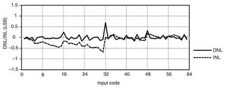
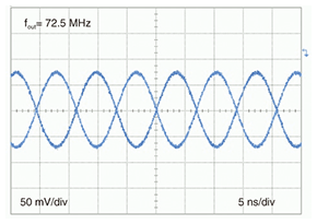
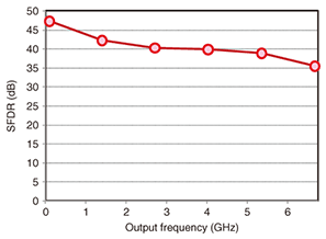
The DAC was tested on-wafer using a probe station and high-frequency probes. It consumes total power of 0.95 W with a supply voltage of –4.0 V. Approximately 75% of the power is consumed by the retiming circuits consisting of the clock and data buffers, clock distributor, D-FFs, and two-stage buffers. The DAC core consumes only 0.24 W. The measured differential nonlinearity (DNL) and integral nonlinearity (INL) are within +0.68/-0.16 LSB and +0.17/-0.68 LSB, respectively, where LSB stands for the least significant bit (Fig. 7). These results demonstrate that the R-2R ladder-based architecture is an appropriate choice for our InP HBT technology to achieve 6-bit resolution. The measured sinusoidal output waveforms for 72.5 MHz at a sampling rate of 13.5 GS/s are shown in Fig. 8. The measured spurious-free dynamic range (SFDR) versus output frequency is summarized in Fig. 9. The SFDR remained above 36 dB up to the Nyquist frequency. These results show that the DAC has very good dynamic linearity over the entire Nyquist bandwidth.
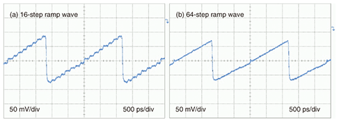
Owing to the limited output data rate of our pulse-pattern generator, we could not measure the dynamic characteristics for a sinusoidal output at rates above 13.5 GS/s. Instead, we measured ramp-wave outputs to characterize the DAC at higher speeds. A ramp-pattern test is often utilized to characterize the dynamic performance of high-speed DACs. The measured 16- and 64-step ramp-wave outputs at a sampling rate of 27 GS/s are shown in Fig. 10. In Fig. 10(a), the 16-step output changed every four sampling-clock cycles, while in Fig. 10(b), the 64-step output changed every sampling-clock cycle. The glitches were well suppressed, and linear ramp-wave outputs were obtained as expected. These results demonstrate that the timing alignment technique works as well as could be expected. The output transient time is less than 20 ps.
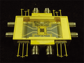
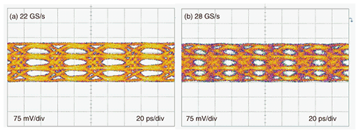
Since the R-2R ladder-based current-steering DAC achieved very good performance, we assembled it into a metal package with high-frequency connectors (Fig. 11) [12] to facilitate its use in an optical transmission experiment. The measured four-level signals for 16-QAM transmission are shown in Fig. 12. The DAC module provided a clear four-level signal with full-scale rise and fall times shorter than 20 ps at a sampling rate of up to 28 GS/s. This DAC module has been used to demonstrate 11 × 171-Gbit/s PDM 16-QAM optical transmission [13]. Thus, this DAC can be applied to post-100-Gbit/s/ch multilevel optical transmission systems.
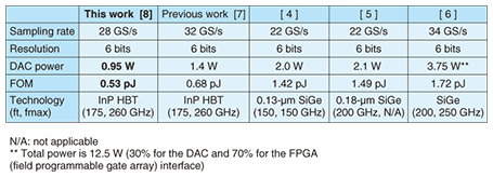
4. ComparisonOur DAC is compared with other state-of-the-art DACs designed for optical transmission systems with a sampling rate above 20 GS/s in Table 1. The figure-of-merit (FOM) for energy per conversion step is defined as where Power is the total power consumption, N is the physical resolution, and fsampling is the maximum sampling rate.
Our DAC shows outstanding performance. It operates at a sampling rate of up to 28 GS/s, consumes only 0.95 W, and has a better FOM (0.53 pJ per conversion step) than any previously reported DACs with sampling rates above 20 GS/s. 5. SummaryIn this article, we presented the circuit design and measured performance of a high-speed low-power DAC using InP HBT technology. To achieve both high-speed and low-power operation, we used a simple R-2R ladder-based current-steering architecture and devised a new timing alignment technique. The 6-bit DAC with timing alignment can operate at a sampling rate of up to 28 GS/s, consumes only 0.95 W, and has a better FOM (0.53 pJ per conversion step) than any previously reported DACs with sampling rates above 20 GS/s. It provides a clear multilevel modulated signal for QAM transmission and can be applied to post-100-Gbit/s/ch 16-QAM systems. Our DAC will be effective for next-generation optical transmission systems. References
|
||||||||||||||||||||||||||||||||