|
|||||||||||||||||||||||||||||||
|
|
|||||||||||||||||||||||||||||||
       |
Feature Articles: Collaborations with Universities Leading to Open Innovation in NTT's R&D Vol. 9, No. 10, pp. 17–23, Oct. 2011. https://doi.org/10.53829/ntr201110fa2 Room-temperature Resonant-tunneling-diode Terahertz Oscillator Based on Precisely Controlled Semiconductor Epitaxial Growth TechnologyAbstractThis article presents the recent achievement of fundamental oscillations in resonant tunneling diodes (RTDs) above 1 THz at room temperature. One of the key technologies for this achievement is precisely controlled epitaxial growth of ultrathin semiconductor heterostructures. The structural design of oscillators and microfabrication technology are also crucial. To increase the oscillation frequency toward the terahertz range, we devised a novel RTD structure with a graded emitter, which effectively reduces both the operating bias voltage and electron transit time in the collector depletion region. An InP-based InGaAs/AlAs RTD oscillator with a graded emitter and 1.2-nm-thick barriers exhibited fundamental oscillations with frequencies of up to 1.04 THz at room temperature, which is the highest oscillation frequency ever reported in single solid-state electron devices. This project is part of collaborative research and development between NTT and Tokyo Institute of Technology. 
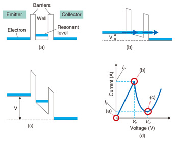
1. IntroductionThe resonant tunneling diode (RTD) is a quantum-effect semiconductor device using quantum mechanical tunneling. Its operating principle is based on the resonant tunneling effect proposed by Tsu and Esaki in 1973 [1]. The conduction-band profiles of a conventional RTD and their relation to current-voltage characteristics are schematically shown in Fig. 1. The case under zero bias is shown in Fig. 1(a). The RTD’s active layers consist of a double barrier (DB) structure where an undoped quantum well layer is sandwiched between two undoped barrier layers. Owing to the use of the quantum mechanical behavior of carriers, each layer of the DB structure is usually on the order of 1 nm thick. The DB layers are connected with heavily doped emitter and collector contact regions filled with electrons. Discrete quasi-bound or resonant levels are formed in the well layer. In Fig. 1(a), the lowest resonant level is indicated. As the bias voltage increases, electrons flow from the emitter to the collector through the resonant level. The current increases almost linearly until the emitter’s conduction band edge exceeds the resonant level, as shown in Fig. 1(b). A further increase in the bias voltage causes a sharp drop in the current because the resonant level falls below the emitter’s conduction band edge, as shown in Fig. 1(c). The current-voltage characteristics in Fig. 1(d) exhibit negative differential conductance (NDC), which is one of the distinctive features of RTDs. The ratio of peak current to valley current (IP/IV) in Fig. 1(d) is called the peak-to-valley ratio (PVR) and is one of the figures of merit of RTDs.
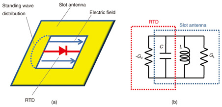
One practical application of such NDC devices is a high-frequency oscillator, which can be constructed by connecting NDC devices and external resonators. The fundamental oscillator structure used in this work, which has an RTD integrated with a slot antenna [2], is shown in Fig. 2. The RTD’s NDC provides the gain necessary for the oscillation. The slot forms a standing wave of the electromagnetic field as a resonator and also acts as an antenna by radiating output power at the same time. The equivalent circuit for the structure in Fig. 2(a) is shown in Fig. 2(b). Here, some of the parasitic elements such as contact resistance have been omitted. Oscillation takes place if Gd > GL, i.e., the NDC’s absolute value exceeds the slot antenna’s radiation loss. The oscillation frequency is determined by the parallel resonance of L and C in Fig. 2(b) corresponding to the standing wave in Fig. 2(a), where inductance L is dominantly produced by the antenna, and capacitance C is produced by the RTD and antenna.
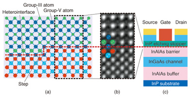
The RTD’s high-speed operation is based on some of the RTD’s distinctive features. One is the short resonant tunneling time, which corresponds to the quantum-mechanical tunneling time of an electron passing through the DB structure; this is estimated to be on the order of 1 ps or less. Another is the short charging time of its own capacitance. The RTD’s high current density of over 1 × 10⁵ A/cm2 and comparatively small capacitance effectively reduce the charging time. These are quite a contrast to other NDC devices such as Esaki diodes where high current density is associated with high doping in the active region, which significantly increases their capacitance and charging time. In the early stage of research, such excellent features of the RTD indicated that RTD oscillators could operate at frequencies never reached by other semiconductor devices. The first demonstration of an RTD oscillator was reported by Sollner in 1984 for GaAs/AlGaAs RTDs; the oscillation frequency was 18 GHz at 200 K [3]. The oscillation frequency reached 712 GHz at room temperature in 1991 with InAs/AlSb RTDs [4]. Recently, the sub-terahertz (sub-THz) and terahertz (THz) ranges have been attracting a lot of interest since there are various potential practical applications such as broadband wireless communications, safety, and security. Although the demands for room-temperature devices operating in the sub-THz to THz range increased, no further increases in RTD oscillation frequency were reported until 2009. Room-temperature operation in the THz range has not yet been achieved in any other single devices. NTT Photonics Laboratories and Tokyo Institute of Technology (Tokyo Tech) have been collaborating on RTD THz oscillator development since 2007. NTT has developed a precisely controlled epitaxial growth technique to obtain high-quality ultrathin semiconductor heterostructures [5]. Tokyo Tech has developed design and microfabrication technology for RTD oscillators operating in the sub-THz to THz range [6]. In 2009, we reported a record-breaking fundamental oscillation at 831 GHz [7]. Last year, we successfully extended the fundamental oscillation frequency to above 1 THz at room temperature [8]. In this article, we present essential technologies for the achievement. Precisely controlled semiconductor epitaxial growth technology developed in NTT and its application to ultrahigh-speed electron devices are described. The design and microfabrication technology for RTD oscillators developed by Tokyo Tech is also presented. Finally, our approach to THz oscillation and its experimental demonstration are shown. 2. Precise control of semiconductor epitaxial growth for ultrathin heterostructures in ultrahigh-speed electron devicesThe atomic configuration of an ideal III-V semiconductor heterointerface is schematically shown in Fig. 3(a). The RTD’s DB structure consists of such heterointerfaces between barrier and well. Good crystal quality for such a heterostructure is essential for modern semiconductor devices, such as high-speed transistors, lasers, and photodiodes, to produce high performance. For example, excellent abruptness of the layer composition is required in actual devices to form an ideal band profile. In Fig. 3(a), the atomic composition changes abruptly at the interface, and there is no mixing layer around the interface. Control of the layer thickness on the order of 1 nm or less is also required. In addition, heterointerface flatness is also important for device performance since actual heterointerfaces often include a high density of monolayer steps, which often affect carrier transport. These III-V semiconductor heterostructures are usually fabricated by an epitaxial growth technique such as molecular beam epitaxy (MBE) or metalorganic vapor-phase epitaxy (MOVPE), in which semiconductor epitaxial layers are grown by depositing source materials on substrates. In NTT Photonics Labs, MOVPE is mainly developed for advanced semiconductor devices for broadband communication systems. In MOVPE, organic metals and hydrides are used as precursors and supplied to the substrate during epitaxial growth. For the fabrication of high-quality heterostructures, control of precursor-supply switching is one of the key procedures. NTT has developed such key techniques and fabricated high-quality heterostructures for practical devices. A high-angle annular dark-field (HAADF) scanning transmission electron microscope (STEM) image of the InP/InAlAs heterointerface in an InP-based high-electron mobility transistor (HEMT) developed in NTT is shown in Fig. 3(b). The HEMT’s layer structure is shown in Fig. 3(c). In Fig. 3(b), each bright dot corresponds to a group-III or group-V atom. It should be noted that the brightness of dots corresponding to group-V atoms changes abruptly at the interface, which means that the distribution of group-V atoms changes abruptly from arsenic to phosphorus. This HAADF-STEM image demonstrates our excellent control of compositional abruptness at the heterointerface. The abruptness provides high wet-etching selectivity in the device fabrication process and contributes to excellent device characteristics. InP-based HEMT integrated circuits based on our MOVPE technology have been used in a 120-GHz advanced broadband wireless communication system [9].
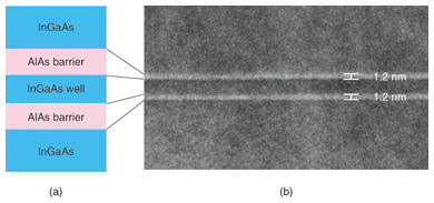
NTT has applied such epitaxial growth techniques to the fabrication of high-performance RTDs. We used InP-based InGaAs/AlAs DB structures because the large conduction-band offset between InGaAs and AlAs is beneficial to obtain a large PVR. Oscillation in the THz region requires peak current density (JP) of around 1 × 10⁶ A/cm2 or more with a large PVR. We have demonstrated precise control of a barrier thickness of around 1 nm and the formation of high-quality heterointerfaces with excellent compositional abruptness and flatness [10]. An example of a cross-sectional TEM image of our RTD is shown in Fig. 4. The image shows the uniformity of 1.2-nm-thick barriers and the smoothness of the heterointerfaces. We have also confirmed excellent on-wafer uniformity on a 3-inch wafer where the barrier-thickness fluctuation was estimated to be around ±0.1 monolayers.
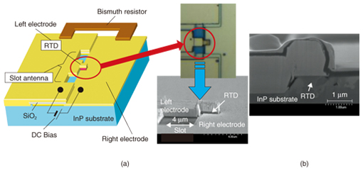
3. Fundamental oscillation above 1 THz at room temperatureSchematic drawings and microscope images of an actual RTD oscillator integrated with a slot antenna are shown in Fig. 5(a). The structures are based on Tokyo Tech’s advanced semiconductor microfabrication technology. The RTD’s electrodes are connected to the antenna’s left and right electrodes. At both edges of the antenna, the electrodes are overlapped with a SiO2 layer between them. This structure forms reflectors of high-frequency electromagnetic waves, and DC bias separation is achieved at the same time. A resistor made of bismuth film is connected in parallel outside the antenna electrodes to suppress parasitic oscillation caused by the resonance formed by external circuits including the bias supplying lines. A cross-sectional image of the RTD oscillator is shown in Fig. 5(b). The RTD’s emitter mesa area is around 1 µm2 or less. The emitter mesa area and slot antenna length are key structural parameters that determine the oscillation frequency and they were carefully designed to increase the oscillation frequency.
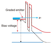
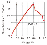
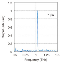
We have improved the RTD’s layer structure to extend the oscillation frequency toward the THz range. The structural-parameter dependences of RTD characteristics, such as the effect of barrier thickness reduction, have been investigated to obtain high JP and reduce the resonant tunneling time. In addition, our previous research revealed that lowering the operating bias voltage of the oscillator is important in order to reduce the electron transit time in the collector depletion region because a low operating bias voltage should suppress electronic transition from G to the L valley, which leads to a decrease in electron velocity [11]. To reduce the operating bias voltage, we have proposed a novel RTD structure with an undoped graded emitter. The conduction band profiles of the DB regions in RTD oscillators with and without a graded emitter at around the operating bias voltage are shown in Fig. 6. Inserting a graded emitter, which consists of Ga-rich InGaAs and forms potential steps at the DB structure’s emitter side, effectively reduced the operating bias voltage. We examined the effectiveness of barrier thickness reduction and graded emitter insertion. An example of the current-voltage characteristics of this novel RTD with 1.2-nm-thick barriers and a graded emitter is shown in Fig. 7. We have successfully obtained an extremely high JP of 2.4 × 10⁶ A/cm2 with a PVR of 2 under a comparatively low bias voltage of 0.8 V. To our knowledge, this is the highest JP ever reported. The current-voltage characteristics indicate the formation of high-quality ultrathin barriers and heterointerfaces. The RTD oscillator’s measured spectrum for fundamental oscillation at 1.04 THz, which is the highest oscillation frequency ever reported in a single solid-state device operating at room temperature, is shown in Fig. 8. The output power was 7 µW. Further optimization of the structural parameters should enable increases in the oscillation frequency and output power to meet the demand for practical compact THz devices.
4. ConclusionsNTT and Tokyo Tech have had great success in their collaborative development of RTD THz oscillators. Using precisely controlled semiconductor epitaxial growth and microfabrication technologies, we have achieved fundamental oscillations above 1 THz at room temperature through optimization of the RTD layer structure. Further increases in oscillation frequency and output power are expected through further improvement of the oscillator structures, which should lead to a practical room-temperature compact THz light source. References
|
||||||||||||||||||||||||||||||