|
||||||||||||||||||||||||
|
|
||||||||||||||||||||||||
       |
Feature Articles: Collaborations with Universities Leading to Open Innovation in NTT's R&D Vol. 9, No. 10, pp. 35–38, Oct. 2011. https://doi.org/10.53829/ntr201110fa5 CMOS LSI for Brain-machine Interface Used in Bidirectional CommunicationAbstractWe introduce our approach to making an LSI (large-scale integration) chip for a brain-machine interface by integrating neuroscience technology developed in NTT Basic Research Laboratories (NTT BRL) with LSI chip design and simulation techniques of Keio University. This LSI contains everything required for bidirectional communication, which enables the brain-machine interface to communicate with the brain on the molecular level when it is combined with a nano-bio device developed in BRL. 
1. IntroductionA brain-machine interface (BMI) links the external world and the neural circuits in the brain, as shown in Fig. 1. The feasibility of communication between the brain and the external world was demonstrated by Wilder Penfield, a Canadian brain surgeon, in the 1930s and 1940s [1]. He stated that “in the course of operations on the brain, electrical stimulation of the human brain, while patients are conscious, has sometimes activated the neuronal record of past experience.” [2]. These findings suggest not only that there may be a correlation between the brain and memory but also that the brain may be accessible from the external world. With today’s technology, neural activity is commonly evoked by electrical, magnetic, and chemical stimulation. Studies related to controlling a robot or computer by using information in the brain made progress at around the end of the twentieth century. Chapin et al. showed that a robot arm can be controlled by neural activity in the cortices of a rat [3] and monkey [4]. Recently, BMI technology has been used for communication and device control for people with severe motor disabilities [5].
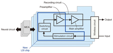
2. Collaboration with Keio UniversityNTT Basic Research Laboratories (NTT BRL) has studied information transmission of neurons, especially in the central nervous system. We have revealed that neural activity in neurons cultured on a planar multielectrode array (MEA) is influenced by electrical stimulation with an MEA-based multisite stimulation and recording system [6]. Although this system was optimized for in vivo experiments, it is applicable to the BMI if the system is miniaturized. On the other hand, the Nakano Lab. in Keio University has studied the design and simulation of an LSI chip that consolidates analog and digital circuits. Since 2008, we have been collaborating to achieve a BMI by combining these technologies through the intermediation and constant encouragement of the Liaison Council of NTT Corporation and Keio University. 3. LSI chip and MEA3.1 Design and functionThe human brain is thought to have more than one hundred billion neurons. Each neuron receives synaptic inputs from several thousand other neurons. A single neuron alone cannot evoke the electrical signals that are called action potentials. Furthermore, electroencephalography shows that local activity in the cerebral cortex is high when the brain processes information. This information processing in the brain is produced through the cooperation of many neurons. So the MEA is suitable for use with a BMI that requires parallel information processing. We have developed a complementary metal-oxide-semiconductor (CMOS) LSI chip with 8-channel preamplifiers for data recording and a stimulus generating circuit [6] based on a multisite stimulation and recording system [7]. The selection of the stimulation sites, their timing, and the applied stimulus waveforms are programmable, which results in vibration-free selection of any combination of the eight electrodes (the MEA) for stimulation. A block diagram of the final form of this LSI chip together with the MEA is shown in Fig. 2. The LSI chip consists of four parts: 1) a recording circuit for measuring neural activity, 2) a stimulation circuit for generating and applying a stimulus signal, 3) a switching circuit and 4) a wireless circuit. The first three circuits are on a 2.5 mm × 1.4 mm chip fabricated by the CMOS process. We are now developing packaging for the main amplifier in the recording circuit and the wireless circuit.
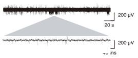
3.2 StimulationInformation from the external world is input to this LSI chip by time-division multiplexing of eight channels by using a 4-bit digital parallel-to-serial converter. This makes it possible to stimulate multisite channels independently. The maximum voltage output is ±700 mV with a biphasic waveform and the minimum pulse width is 20 µs. 3.3 Neural activity measurementThe neural activity of dissociated rat cortical neurons (embryonic day 18) cultured on a planar MEA (40 days in vitro) is shown in Fig. 3. The neural activity, which was measured as voltage signals with the LSI chip via the MEA, was relatively small compared with the noise level. The noise comes from lines between a preamplifier and an electrode because it is difficult to seal them. So the noise level depends on the lengths of these lines. An LSI chip with a preamplifier allows a shorter line length when it is mounted near the MEA. Moreover, it can evoke neural activity and measure it through the same electrode by switching the stimulation and recording circuits. These characteristics make it a suitable device for enabling a BMI to be attached to a body and exchange information via an MEA with low noise.
4. Interface for nano-bio deviceNeural information is transmitted by means of the action potential in one neuron and chemical signals between two neurons across a synapse. When the action potential arrives at a synapse called a presynaptic terminal, a chemical substance called a neurotransmitter is released. Neurotransmitters bind receptor channels on a neighboring neuron called a postsynaptic neuron. Then, receptor channels open and the current flow carried by ions enters and exits through the receptor channels. When depolarization of the postsynaptic neuron as a result of the current flow reaches a certain threshold, an action potential is generated in the postsynaptic neuron. Recently, nanotechnology has attracted attention in industrial, medical, and scientific fields. In the field of neuroscience, this technology enables access from one neuron to one protein molecule such as a receptor channel, which is an essential component for neural information transmission. NTT BRL has studied an artificial synapse for accessing neural information by means of a silicon substrate by integrating nanotechnology and biotechnology [8]. The silicon substrate has microwells covered with a lipid bilayer containing reconstituted membrane proteins. This device emulates the functions of a postsynaptic membrane and lets us measure chemical signals as electric signals when electrodes are installed on the two sides of the lipid bilayer. 5. ConclusionsAn LSI chip integrated with an artificial synapse enables communication with neurons at the biomolecular level. This feature could provide an alternative function for patients with nervous diseases or a new tool for discovering drugs that act directly on receptors. AcknowledgmentsThis work is supported by the VLSI Design and Education Center of the University of Tokyo in collaboration with Cadence Design Systems, Inc. References
|
|||||||||||||||||||||||