|
|||||||||||||||||||
|
|
|||||||||||||||||||
       |
Feature Articles: Optical Semiconductor Technologies for Photonic Networks Vol. 10, No. 12, pp. 50–55, Dec. 2012. https://doi.org/10.53829/ntr201212fa8 High-speed Photodetector TechnologiesAbstractWe have developed several kinds of high-speed photodetector technologies for broadband photonic networks. This article reviews three of NTT's high-speed photodiodes: ultrahigh-speed photodiodes, specially designed photodiodes with high responsivity and low operating voltage, and avalanche photodiodes.
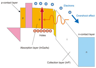
1. IntroductionBecause of the popularity of the Internet and video-on-demand services, the capacity of photonic network systems must be continuously increased. A semiconductor photodetector, which converts an optical signal into an electrical signal, is a key device in receivers in photonic network systems. The general demands for photodetectors are faster operating speeds for higher bit-rates, higher efficiency for better sensitivity, and lower operating voltage for lower power consumption by the receiver. In the 1990s, we developed the uni-traveling-carrier photodiode (UTC-PD) structure that makes the best use of electron transport and has the advantages of simultaneous high-speed and high-output operation [1]. Since UTC-PDs can maintain their photodetection function for input signals with frequencies above 1 THz, they have been used as terahertz microwave generators [2]. In the receivers of photonic network systems, high responsivity is also very important to improve receiver sensitivity. To meet this requirement, we have developed the maximized-induced-current photodiode (MIC-PD) by modifying the UTC-PD [3]. The MIC design can maximize the responsivity at a required bandwidth by means of a hybrid (combined p-type and depleted (p: positive semiconductor)) absorption layer. This technology has been successfully applied to photodiodes for 100-Gbit/s receivers of digital coherent transmission systems. Moreover, avalanche photodiodes (APDs), which provide amplification as well as photodetection, are used in access and metro networks and Ethernet. We had already developed APDs for 10-Gbit/s operation but there have recently been requests for high-speed APDs, e.g., for 25-Gbit/s receivers for 100-Gbit/s-based Ethernet. 2. Ultrahigh-speed photodiodes (UTC-PDs)One widely used photodetector is the p-i-n photodiode (pin-PD), which has a depleted absorption layer of intrinsic semiconductor (i-layer) between positively and negatively doped electrode layers (p- and n-type semiconductor layers). In a pin-PD, two types of charge carriers—both negative electrons and positive holes—are photogenerated and contribute to the external induced current. Because holes have a much lower velocity than electrons (1/10 the speed), the device’s response speed is dominated by hole transport. Therefore, we developed the UTC-PD, which can achieve ultrahigh-speed operation, by removing this limiting factor for the pin-PD. As illustrated in Fig. 1, carriers are generated in the p-type absorption layers and only electrons are injected into the depleted carrier collection layer, whose thickness is designed independently of the absorption layer. Since the holes are majority carriers in the p-type absorption layer, their transport is the collective motion with a high response time determined by the dielectric relaxation time. Eventually, only electrons behave as active carriers in the UTC-PD; thus, UTC-PDs can achieve ultrahigh-speed and high-current operation without the space-charge-effect induced by hole accumulation.
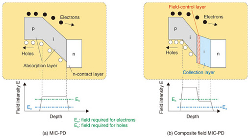
A 3-dB bandwidth (f3dB) of over 300 GHz has been obtained for a UTC-PD. We have developed a UTC-PD-based terahertz photomixer module for frequencies beyond 1 THz [2]. 3. Specially designed PD with high responsivity and low operating voltage: MIC-PDA drawback of the UTC-PD is low responsivity when the absorber has been designed to be relatively thin in order to achieve high-speed operation. To optimize both the response speed and responsivity, we have developed the MIC-PD. In the MIC-PD design, the absorption layer consists of p-type and depleted layers, as shown in Fig. 2. Although there is hole transport contributing to the output current, the thickness of the depleted absorption layer does not have to be as large as in a pin-PD, and it is adjusted to retain the advantage of the high-speed potential of the UTC-PD. This combined p-type and depleted absorption layer allows us to maximize responsivity and operating speed simultaneously. Namely, the responsivity can be higher than that of a UTC-PD with the same bandwidth and the operating speed can be higher than that of a pin-PD with the same responsivity.
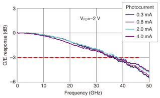
We have developed various MIC-PD structures for advanced photonic network systems. One is a dual polarization quadrature phase shift keying (DP-QPSK) (or digital coherent) system [4], which is now being intensively investigated toward future high-speed, high-capacity optical transmission systems. In this system, the PD is required to operate in a wide bandwidth with a high average photocurrent induced by a high-power local oscillator input. Because a high photocurrent induces a space charge effect in the depletion layer of a PD, bandwidth reduction occurs. To overcome this problem, we have developed a composite-field MIC-PD which can optimize the bandwidth by suppressing the space charge effect even at low bias voltages [5]. The band diagrams and electric field distributions of a conventional MIC-PD and the new composite-field MIC-PD are shown in Figs. 2(a) and (b), respectively. An f3dB of more than 30 GHz is required for a PD in a 100-Gbit/s digital coherent system. To meet these system needs, the thickness of the photoabsorption layer is reduced in order to shorten the carrier-transit time. A thinner absorption layer generally results in higher device capacitance, which reduces the operating speed. However, by incorporating an undoped carrier collection layer of a wide-bandgap material, we were able to widen the depletion width and maintain low junction capacitance. Moreover, an n-type field control layer tailors the step-like field profile, leading to sufficient field for hole transport in the depleted absorber even at a low bias voltage. In the collection layer, only electrons are traveling carriers; here, a low field (10 kV/cm) is sufficient to keep the electron transit time short. An important point is that the field control layer generates a much higher electrical field in the depleted absorption layer and the partial absorber layer suppresses the space charge effect. Consequently, the composite-field MIC-PD allows a lower operating voltage and higher output current with higher responsivity than a conventional PD. The frequency responses of a fabricated composite-field MIC-PD for optical-to-electrical (O/E) conversion with average photocurrents of 0.3 mA, 0.8 mA, 2.0 mA, and 4.0 mA are shown in Fig. 3. The reverse bias voltage supplied to the PD was as low as 2.0 V, which suits the common power supply voltage with a transimpedance amplifier of +3.3 V. The f3dB reached more than 35 GHz for average photocurrent from 0.3 mA to 4.0 mA. We confirmed that there was no degradation in the frequency response caused by the space charge effect up to 4 mA. These good results show that composite-field MIC-PDs are suitable devices for receivers front-end of 100-Gbit/s digital coherent systems.
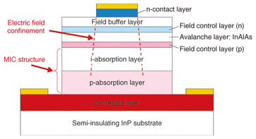
4. High-speed APDsAPDs offer improved responsivity because of the internal gain due to the multiplication of carriers in a high electric field. This function of APDs is very important and they have been used in the 10-Gbit/s metro and access systems. The technology trend is now toward systems with higher bit rates such as the 100-Gbit/s Ethernet system in which the speed of each lane is 25 Gbit/s (25 Gbit/s × 4 channels). For use in such novel high-speed systems, we have developed a new APD with the MIC design [6]. The schematic cross section of our high-speed APD is shown in Fig. 4. The general figure of merit of an APD is expressed by the product of the multiplication factor (M) and f3dB. This product depends on the material and thickness of the avalanche layer. We chose InAlAs as the material to obtain a higher M-f3dB product.
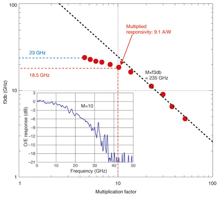
Another feature of our device is that field confinement is achieved by the inverted p-down structure with a top n-contact. Field confinement is very important for device reliability in order to avoid degradation caused by suppression of the leakage current on the surface. Zn diffusion [7] and/or Si-ion implantation [8] are conventionally used for APD fabrication, but we decided not to use them in order to simplify the fabrication process. This simplicity also allows better reproducibility and lower fabrication cost. However, the field confinement becomes the source of edge breakdown at the periphery of the n-contact mesa, which limits operation at a large multiplication factor in active area. To solve this problem, we added a field buffer layer underneath the n-contact layer and n-type field control layer. The variation in f3dB with multiplication factor M is shown in Fig. 5. The maximum value of f3dB was 23 GHz, and it decreased with increasing M. For M higher than 15, f3dB values fell on a straight line, indicating an M-f3dB product of 235 GHz. Owing to the high responsivity achieved the MIC design, high multiplied responsivity of 9.1 A/W was obtained at f3dB of 18.5 GHz.
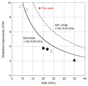
High multiplied responsivity with sufficient bandwidth is important in practical network systems. The present result is compared with previously reported values in Fig. 6. As seen in this figure, the obtained value of 168 GHz A/W for our APD is superior to all other reported ones. Consequently, our APD is a promising candidate for high-speed network systems, e.g., 100-Gbit/s Ethernet systems with 25-Gbit/s operation.
5. ConclusionThe MIC design, which is a modification of the UTC-PD structure, can optimize responsivity and operating speed. MIC-PDs for 100-Gbit/s digital coherent system possess high current capability while maintaining a high f3dB, even at a low bias voltage. Our APD structure is fabricated with an inverted p-down layout to utilize the MIC design and field confinement by a top n-contact mesa. To avoid local breakdown associated with field confinement, a field buffer layer is applied. The best measured multiplied responsivity of 9.1 A/W was obtained at f3dB of 18.5 GHz, which is sufficient performance for 25-Gbit/s operation in 100-Gbit/s Ethernet systems. AcknowledgmentThis work was partly supported by the Ministry of Internal Affairs and Communications of Japan through the R&D project “High-speed Optical Transport System Technologies”. References
|
||||||||||||||||||