|
|||||||||
|
|
|||||||||
       |
Feature Articles: Optical Semiconductor Technologies for Photonic Networks Vol. 10, No. 12, pp. 56–61, Dec. 2012. https://doi.org/10.53829/ntr201212fa9 InGaAs Metamorphic Laser for
|
||||||||
 |
 |
1. Introduction
Network traffic is rapidly increasing and so is the energy consumed by communication systems. Therefore, it is important to find a way to reduce the power consumption of transmitter modules. In an optical transmission module, a temperature controller such as a Peltier device consumes more power than other components. The temperature controller suppresses deviations in laser characteristics such as output power and modulation characteristics, which are sensitive to the ambient temperature. If we can improve the laser's temperature characteristics, we may be able to eliminate the need for a temperature controller, which will allow a significant reduction in power consumption.
In this article, we describe our efforts towards achieving a 1.3-μm-range laser with low power consumption. The 1.3-μm range has zero dispersion and is used for metro, access, and Ethernet systems.
For 1.3- and 1.55-μm-range optical fiber communication light sources, an InGaAsP-based laser has already been used. It is fabricated on an InP substrate and an InGaAsP quantum well is used as the active region. This type of laser performs well at around room temperature; however, an increase in the ambient temperature degrades the output power and the injection current (operating current) increases, as shown in Fig. 1(a). Therefore, a temperature controller has been indispensable and power consumption has been difficult to reduce. There is strong demand for a laser with good temperature characteristics, as shown in Fig. 1(b).
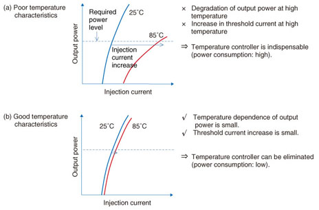
Fig. 1. Temperature characteristics of lasers.
The temperature dependence of a laser can be explained as follows. The laser light is amplified by current injection in a quantum well acting as an active region. As the ambient temperature is increased, the injected electrons tend to overflow from the quantum well into other regions such as the barrier layer, the separately confined heterostructure (SCH), and the cladding layer, as shown in Fig. 2. The electrons that overflow from the quantum well recombine with holes without light emission, which leads to an increase in threshold current at high temperature. Therefore, to stabilize the laser performance against temperature fluctuations, it is necessary to make a deep quantum well that has a large potential gap from the barrier layer.
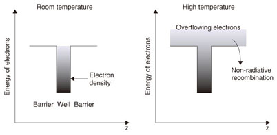
Fig. 2. Degradation mechanism at high temperature (carrier overflow from quantum well).
Several materials used for 1.3-μm-range lasers and their performances are listed in Table 1. With a conventional active region made from InGaAsP-based material on an InP substrate, it is difficult to make deep potential quantum wells and have an operating current at high temperature of over 40 mA at 10 Gbit/s. InGaAlAs-based materials on an InP substrate have been studied with a view to improving the temperature, and they are gradually being used for uncooled light sources. On the other hand, strained InGaAs lasers on a GaAs substrate have superior temperature characteristics to those on an InP substrate because a larger band offset between the cladding and SCH can be selected. However, the critical thickness of a strained quantum well limits the emission wavelength to below 1.2 μm. To overcome this obstacle, InGaAsN quantum wells and InAs quantum dot lasers that provide 1.3-μm emission on a GaAs substrate have been developed. However, their reliability and modulation speed still need to be improved. Another approach is to use a metamorphic buffer on GaAs [1]–[3]. This technique enables us to use materials with a lattice constant between that of InP and GaAs and to make a 1.3-μm-range laser on a GaAs substrate with good temperature characteristics.
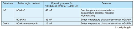
Table 1. Materials for 1.3-μm-range lasers and their performances.
2. Metamorphic growth technique
The metamorphic growth technique allows us to grow a material whose lattice constant is different from that of the substrate. Therefore, we can design the device materials without being constrained by substrate lattice-constant limitations. In this study, we used an InGaAs layer grown on a GaAs substrate under special conditions by metal-organic vapor phase epitaxy (MOVPE). Conventionally, strain relaxation occurs if the strained layer thickness exceeds the critical thickness and threading dislocations appear in the upper layer and the surface tends to become rough. With metamorphic growth, a stable dislocation network is formed in the thin layer between GaAs and the InGaAs buffer layer, which leads to a low threading dislocation density in the upper layer. We can regard this layer as a virtual InGaAs substrate because the strain is fully relaxed and there is little surface roughness. Transmission electron microscope images of a fabricated metamorphic laser are shown in Fig. 3. We confirmed that the dislocations are concentrated at the buffer boundary and the dislocation density is low enough to make a high-performance laser.
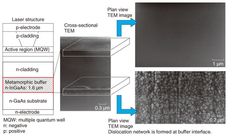
Fig. 3. Transmission electron microscope (TEM) images of metamorphic buffer.
3. Fabrication and characteristics
A schematic of the fabricated metamorphic laser is shown in Fig. 4. The metamorphic buffer consists of n-doped In0.12Ga0.88As 1.6 μm thick (n: negative). The In0.1Ga0.9As layer with reduced indium content on this metamorphic buffer is fully relaxed and acts as a virtual InGaAs substrate. The n-InGaAlAs lower cladding layer is lattice matched to the virtual In0.1Ga0.9As substrate. The active layer consists of three compressive-strained InGaAs quantum wells sandwiched between In0.1Ga0.9As barrier layers. The p-InGaP upper cladding has the same refractive index and lattice constant as the lower n-InGaAlAs cladding (p: positive). We chose InGaAlAs for the lower cladding because it has better surface roughness than InGaP cladding. On the other hand, we chose InGaP for the upper cladding because it has the advantage of letting us make a ridge structure by wet chemical etching. This technique enables a narrow ridge structure and single lateral mode operation. We made and evaluated a Fabry-Pérot-type laser structure.
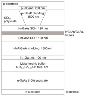
Fig. 4. Schematic of fabricated metamorphic laser.
The temperature dependence of the output power is shown in Fig. 5. This device had a 200-μm-long cavity. One facet had a highly reflective coating and the other was in the as-cleaved condition. Insets show the lasing spectra at various currents at room temperature. We confirmed high output power and lasing at up to 140°C. Eye diagrams obtained with 10-Gbit/s non-return-to-zero direct modulations are shown in Fig. 6. We confirmed clear eye openings from 25°C to 100°C and the potential for making an uncooled light source.
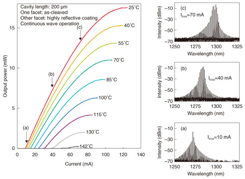
Fig. 5. Temperature dependence of output power and lasing spectra.
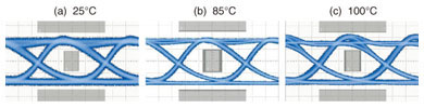
Fig. 6. 10-Gbit/s eye diagrams of metamorphic laser.
4. Improvements in temperature characteristics
As mentioned above, a metamorphic laser consists of materials whose lattice constants are between those of InP and GaAs, so the design is very flexible. We are optimizing the device structure by performing simulations and experiments. Here, we report some of our results. Band diagrams of a metamorphic laser before and after improvement are shown in Fig. 7.
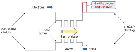
Fig. 7. Band diagrams of improved device using an InGaAlAs electron stopper.
For the cladding materials, we used n-InGaAlAs and p-InGaP for the reasons mentioned above. We newly introduced a p-InGaAlAs layer as an electron stopper into the p-InGaP cladding and obtained improved temperature characteristics.
The temperature dependence of the I-L (injection current versus output light power) characteristics of 1200-μm-long devices is shown in Fig. 8. The temperature dependence of the threshold current was lower than in the case without an electron stopper layer. The maximum operating temperature is as high as 200°C, compared with 175°C for the laser without an electron stopper layer. The characteristic temperature T0, which indicates the threshold increase as a function of temperature, was improved from 80 K to 220 K. T0 at temperatures between T1 and T2 (in °C) is expressed as
Ith(T2) =Ith(T1)·exp ((T2-T1)/T0).
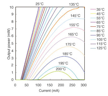
Fig. 8. I-L characteristics of improved devices.
By contrast, a conventional laser on an InP substrate has a characteristic temperature between 50 K and 80 K. With its high characteristic temperature, the metamorphic laser exhibits only a small increase in threshold current at high temperature. Therefore, the operating current for uncooled operation can be reduced, which makes this laser a good candidate for a low-power-consumption light source.
The eye diagram of a 200-μm-long device for direct modulation below 85°C is shown in Fig. 9. The bias current for 10-Gbit/s modulation below 85°C is as low as 15 mA, which is about half the value for a conventional laser on an InP substrate and low-power-consumption operation was confirmed. We believe that this laser can be used as a light source in environments where the temperature exceeds 100°C in an integrated circuit.
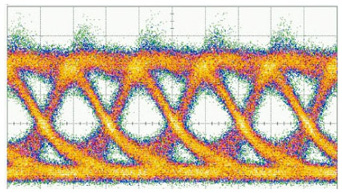
Fig. 9. Eye diagram for improved device for 10-Gbit/s low-bias operation.
5. Concluding remarks
We are conducting trials of low-power-consumption light sources using a metamorphic laser. This laser offers high-speed operation and good temperature characteristics, which enable it to operate with low power consumption. In the future, we will apply this technique to a distributed feedback laser and integration with other types of substrates.
References
| [1] | T. Uchida, H. Kurakake, H. Soda, and S. Yamazaki, "1.3 µm InGaAs/GaAs strained quantum well lasers with InGaP cladding layer," Electron. Lett., Vol. 30, No. 7, pp. 563–565, 1994. |
|---|---|
| [2] | I. Tångring, S. M. Wang, M. Sadeghi, A. Larsson, and X. D. Wang, "Metamorphic growth of 1.25–1.29 µm InGaAs quantum well lasers on GaAs by molecular beam epitaxy," Journal of Crystal Growth, Vol. 301–302, pp. 971–974, 2007. |
| [3] | M. Arai, T. Fujisawa, W. Kobayashi, K. Nakashima, M. Yuda, and Y. Kondo, "High-temperature operation of 1.26 μm Fabry-Perot laser with InGaAs metamorphic buffer on GaAs substrate," Electron Lett., Vol. 44, No. 23, pp. 1359−1360, 2008. |