|
|||||||||||||
|
|
|||||||||||||
       |
Feature Articles: Circuit and Device Technologies for Extremely Low-power Consumption for Future Communications Systems Vol. 11, No. 2, pp. 11–17, Feb. 2013. https://doi.org/10.53829/ntr201302fa2 Low-power LSI Techniques for Next-generation FTTH SystemAbstractDemand for reduced power consumption of network devices is growing as Internet protocol traffic increases and fiber-to-the-home service penetration expands. This article describes our low-power-consumption technology developed for application to medium access control large-scale integrated circuits (LSIs) and analog front-end integrated circuits. Power saving is achieved with dynamic control according to the traffic state or link state, which reduces power consumption in LSIs and in entire network systems.
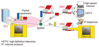
1. IntroductionThe number of fiber-to-the-home (FTTH) subscribers in Japan has reached more than 20 million, and the volume of downstream traffic is now as high as 1.7 Tbit/s [1]. The Gigabit Ethernet passive optical network (GE-PON) is widely used as the main access network. The expansion of cloud computing applications, 3D (three dimensional) video, and high-definition video (4K video) will likely lead to further increases in Internet traffic. The deployment of 10G-EPON, which is ten times faster than GE-PON, is expected in order to handle the increasing volume of traffic. The international standard for the 10G-EPON physical link layer (IEEE 802.3av) [2] was established in 2009. System-level 10G-EPON standards (IEEE 1904.1 SIEPON) are now being studied, with completion aimed for in 2013. An overview of the 10G-EPON system is shown in Fig. 1. An optical line terminal (OLT) is located at a central office, and several optical network units (ONUs) are installed at each user premises. The ONUs share the optical fiber connected to the OLT through a splitter. The OLT must support 10G and 1G dual-rate communications to accommodate the coexistence of three different types of ONUs: symmetric 10G ONUs, asymmetric 10G ONUs, and 1G ONUs.
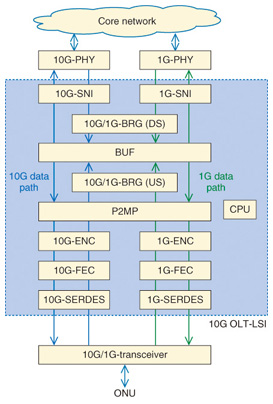
Reducing the power consumption of access network systems is a pressing issue. ONU power consumption accounts for 60% of power consumed by the entire network, including the Internet protocol (IP) core network, because the number of ONUs is proportional to the number of subscribers. The power consumption of access networks accounts for more than 80% of the total network power consumption, including the OLT and aggregation network switches. In the 10G-EPON system, the need for dual-rate burst lG/10G reception will lead to an increase in hardware scale and power consumption. Nevertheless, the dual-rate reception is necessary in order to accommodate the existing GE-PON, which will allow the coexistence of 10G and 1G data paths, and to accommodate multiple forward error correction (FEC) and encryption methods for 10G and 1G data communications. The following techniques for reducing the power consumption of a practical 10G-EPON system are therefore very important. - Reducing the number of transistors and the power consumption of LSI devices - Downsizing and reducing the power of the system by incorporating peripheral components into large-scale integrated circuits (LSIs) - Controlling the power consumption of devices according to the traffic and operating status 2. 10G-EPON medium access control (MAC) LSI2.1 ArchitectureWe have developed a chipset for the dual-rate 10G/1G EPON OLT MAC control LSI and the symmetric/asymmetric supporting 10G-EPON ONU MAC control LSI, which integrates all functions specified in the IEEE 802.3av standard in 40-nm complementary metal oxide semiconductor (CMOS) technology for the first time. A block diagram of the dual-rate 10G/1G EPON OLT is shown in Fig. 2.
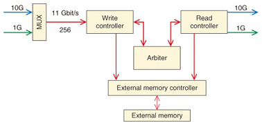
The OLT LSI can independently transmit 10- and 1-Gbit/s frames through two system network interfaces (SNIs) for 10 and 1 Gbit/s data rates with a core network. In this OLT LSI, 10-Gbit/s frames are deserialized to a 64-bit width at 156 MHz, and 1-Gbit/s frames are deserialized to an 8-bit width at 125 MHz. Then both the 10G and 1G frames are transferred to the bridge block (BRG). In the BRG and buffer block (BUF), 10G and 1G data paths are multiplexed, and frame operations such as priority control and destination search are performed. The point-to-multipoint link control block (P2MP) manages and controls the link status of the connected ONUs and grants permission for upstream transmission to the ONUs. The P2MP also controls the frame reception timing of burst upstream signals, so it is considered to be the heart of the LSI. Thereafter, the LSI is connected to a 10G/1G dual-rate transceiver through the encryption block (ENC), forward error correction block (FEC), and serializer-deserializer block (SERDES), which converts the multiplicity of input/output signals. The 1G and 10G data paths are separated at the FEC and ENC blocks because the standard specifications for FEC and encryption are different for 1G and 10G. In contrast, the data paths for 1G and 10G are shared at the BRG and BUF blocks in order to reduce the size of the BRG and BUF circuits. 2.2 Downsizing of encryption circuitTo distinguish and receive 1G burst signals from asymmetric 10G-ONUs and conventional 1G-ONUs, an encryption method must be selected, and decryption must be properly performed. If we employ a method that distinguishes the decryption algorithms by examining the received frame, the OLT has to buffer the frame during the time it takes to examine it and dynamically select the algorithm. This requires an additional frame buffer and increases the OLT latency. The OLT already knows the upstream receive time slot and the type of source ONU because the OLT assigns the bandwidth for ONUs so that upstream frames from each one do not overlap each other. The decryption controller we implemented can evaluate decryption methods and set up the decryption algorithm before the frames are received. The dynamic bandwidth allocation information-based scheduling method eliminates the need for additional upstream-frame buffering and makes it possible to change the decryption algorithm burst by burst. Not only can significant hardware overhead be avoided but also the increase in latency can be suppressed. 2.3 High-throughput data-path constructionThe details of the BUF block are depicted in Fig. 3. A 10-Gbit/s data path and a 1-Gbit/s data path are multiplexed in the multiplexer (MUX) to a 256-bit width. This is because throughput greater than 22-Gbit/s for the read and write operations of memory access is necessary for full wire-rate transmission. In addition, to prevent throughput degradation by continuously writing short frames such as 64-byte frames to memory, a memory write controller writes frames to external memories only when more than 1 kbyte of frame data is stored in the buffer memory in the write controller. Frames of both 10G and 1G data are first stored in the same buffer memory and then sent from the buffer in the order of priority determined by the BRG block. In this way, we reduce the number of external memories and the size of the circuits, and we suppress the delay.
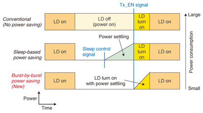
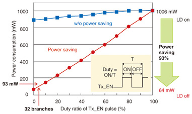
2.4 Flexible functionalityThe OLT P2MP manages the states of ONUs such as the link state and power-saving state. The OLT or ONU transmits and receives the control frame to and from each other and changes their state. To prevent signals from the ONUs colliding in the upstream, the OLT distributes the timing in 16-ns clock order to all ONUs for synchronization. The main functions of the P2MP are as follows: - Carrying out multiplexing and demultiplexing in order to send and receive data frames and control frames. - Generating local reference time and controlling signals for each block in the LSI - Managing the ONUs, including link-status monitoring, control-frame generation and transmission, and control-frame reception and parsing. To allow the 10G-EPON systems to be adapted to various services such as triple play or bandwidth-guarantee, the P2MP block should be able to perform protocol processing between the ONU and OLT with extendibility and flexibility. Moreover, flexible protocol processing can support effective ONU sleep management to save power. Software-hardware cooperation in protocol processing is an efficient way to achieve extendibility and flexibility. The function which needs precise control for maintaining the timing accuracy and throughput requirements was extracted as a hardware execution function. By contrast, flexible ONU management is assigned to software. This assignment enables the P2MP to modify the management of each ONU state and transmit control frames with any format. Thus, the OLT with traffic control and link status monitoring implemented in software enables us to achieve ONU sleep management for power saving. 3. Burst-mode laser diode driver (BLDD)3.1 Power consumption of burst-mode transmitterReducing power consumption is a pressing need for the burst-mode transmitter because 10–20% of the ONU power is consumed by the BLDD. A simple approach for power saving is to shut down the transmitter when there are no upstream optical bursts. However, this approach can be applied only during long periods of no data transmission because of the long settling time [3]. When a PON system has 32 branches, the maximum number allowed by IEEE 802.3av, each laser diode (LD) can be turned off for 97% (= 31/32) of the time on average. The conventional BLDD consumes power continuously irrespective of the existence of traffic. The sleep-based power saving requires a settling time to power up, and a sleep control signal is required in addition to the transmit enable (Tx_EN) signal currently used as the standard. The transmitter receives the Tx_EN signal from the PON control IC and turns on the LD after power is recovered. In our burst-by-burst power saving scheme, both the power and LD turn on simultaneously when the Tx_EN signal is received (Fig. 4). Our proposed BLDD can exploit the short absence of transmission data by shortening the power settling time to approximately 3% of the maximum LD turn-on delay of 512 ns defined in IEEE 802.3av, thereby saving power efficiently.
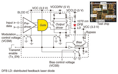
3.2 BLDD with power-saving featureA block diagram of the proposed BLDD circuit and a photograph of a test chip that was designed and fabricated in 0.18-μm SiGe BiCMOS (bipolar CMOS) technology are shown in Fig. 5. To quickly restore power from the power-saving mode, a current switch is added to the current source of each block. The gate circuit is put in the front stage of the output driver to keep the input signal at the differential low level when the laser is off with power saving. Maintaining the input at a low level makes the laser extinction more reliable. The gate circuit has to act as a pre-buffer for the large output driver and therefore consumes a relatively large current when the laser is on. However, because the low-level output does not need a large bandwidth, we are able to implement a mechanism in the gate circuit that allows the circuit to reduce power consumption itself during the LD-off state. The combination of burst control mechanisms and current switching enables both effective power saving and complete extinction of the laser [4], [5]. The distinctive feature is that both the burst operation and power saving are controlled by only a single Tx_EN signal.
The input data stream for all measurements was a 231-1 PRBS (pseudo-random bit sequence) NRZ (non-return-to-zero) signal with a data rate of 10.3125 Gbit/s. The measured power consumption for burst-by-burst power saving operation and conventional non-power-saving burst operation with various duty ratios of Tx_EN signal pulsing are shown in Fig. 6. The Tx_EN pulse frequency was 2 MHz. The power consumption is dramatically reduced from 1006 to 64 mW when the laser is turned off with the power-saving operation. In contrast, the change in power consumption for the conventional burst operation is very small. Our BLDD reduces power consumption by more than 90% when the PON system has 32 branches.
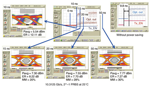
The transient optical waveforms after fourth-order Bessel-Thomson filtering with the burst-by-burst power saving operation are shown in Fig. 7. The waveforms were measured 10, 15, 20, and 50 ns after the transmission was enabled. The BLDD demonstrates a sufficient average optical launch power of 7.3 dBm, an extinction ratio of 8.22 dB, and a mask margin of 20% at 15 ns. The mask margin increases to 30% at 50 ns. These results show that our BLDD quickly recovers from the power-saving mode in 15 ns or less, which is 34 times faster than the turn-on time defined in IEEE 802.3av PR30 standards. Without power saving, the turn-on time is 9.8 ns, which means the penalty for the power saving is under 6 ns. This is the first burst-by-burst power saving circuit that satisfies the IEEE standard with a sufficient margin.
4. ConclusionWe introduced techniques for designing MAC LSIs and burst-mode laser driver ICs to achieve power saving in the 10G-EPON system. The increase in communications traffic is expected to continue, which will inevitably result in equipment becoming larger. To control power saving of an entire system, electric power control for power saving at the LSI level and cooperative operation between many connected LSIs and ICs are needed. We will work on implementing a control mechanism for LSIs to achieve such system-level power saving. References
|
||||||||||||