|
|||||||||||||||||
|
|
|||||||||||||||||
       |
Feature Articles: Circuit and Device Technologies for Extremely Low-power Consumption for Future Communications Systems Vol. 11, No. 2, pp. 23–28, Feb. 2013. https://doi.org/10.53829/ntr201302fa4 Nanowatt Circuit Technology for an Ultrasmall Wireless Sensor Node with Energy HarvesterAbstractThis article describes an ultrasmall wireless sensor node (WSN) that is powered by an energy harvester. The small WSNs can be mounted on any kind of object without increasing their volume, and the energy harvester provides power without having to worry about battery life. However, it is difficult to achieve a WSN that is both ultrasmall and yet still has sufficient power; the smaller the energy harvester is, the less power it generates. We have developed two nanowatt circuit techniques to address this issue. One is a sensing circuit that converts signals with vibration energy. The other is a wireless circuit that uses a quick startup ring oscillator and pulse modulation with an intermittent-driving radio frequency circuit.
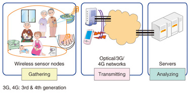
1. IntroductionWireless sensor networks that can gather and analyze trivial information such as vibration, temperature, angles, or positions will lead to the development of new services [1]–[4]. For example, a current sensor attached to electrical appliances in a house can detect how much electricity is used or saved over time, and a sensor that can detect patterns in vibrations caused by wind can indicate cracks in concrete structures. In addition, wireless sensor networks make it possible to provide machine-to-machine (M2M) networks where appliances operate voluntarily without human instructions. An image of a wireless sensor network is shown in Fig. 1. The network consists of wireless sensor nodes (WSNs) that can be mounted on any object or living thing to monitor environmental or physical conditions, on master receivers that are connected to the network to collect information from the WSNs, and on servers to store and analyze data.
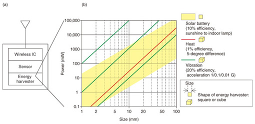
Our concept is to make the WSNs ultrasmall and to drive them with an energy harvester. The small WSNs can be mounted on any object without increasing the object’s volume. The energy harvester draws ambient energy from the surrounding environment. This means that the conventional battery is unnecessary as a power source, and consequently, there are no concerns about battery life. These two aspects also reduce the cost of the WSNs and make them less intrusive, which allows a greater range of applications. Unfortunately, there is a conflict between energy harvesting and node miniaturization; as the energy generator becomes smaller, so does the generated power. In this article, we describe ultralow power, nanowatt circuit technology that we developed to address this problem. This article is organized as follows. Section 2 describes the energy harvester and nanowatt circuit technology. Section 3 covers the components and circuits of the WSN, and section 4 concludes the article. 2. Nanowatt circuit technologyThe minimum configuration of the WSN energy harvester, sensor, and wireless integrated circuit (IC) is shown in Fig. 2(a). We first discuss the energy harvester and then explain the sensing circuit and the wireless configuration.
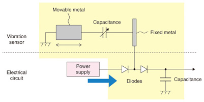
2.1 Energy harvesterThe size of the energy harvester versus the energy generated from ambient heat, vibration, and light sources is shown in Fig. 2(b) [5]. The shape of the solar battery is considered as a square, and the others as cubes. Naturally, more energy degradation occurs as the size of the harvester decreases. The energy source that is selected therefore depends on the usage conditions and energy requirements. For example, there is a good source of heat when WSNs are mounted on human skin or on a large-scale integrated circuit (LSI) of a computer. However, the energy conversion efficiency is low in this case, and a heat waste structure is needed to convert energy. Vibration is a good energy source for WSNs mounted on humans or vehicles, but space is needed for the vibration generator. Further, the vibration frequency depends on the shape and the material of the generator, which limits the flexibility for modeling the generator. Light is a good energy source only when the light is irradiated. The generated power is affected by the light source, and the intensity of light in different environments, for example, a dark wine cellar, and a sandy beach on a sunny day, can vary dramatically. Whichever energy source is chosen, the generated power for a WSN less than 1 cm in size under stable conditions, such as when there is no one in a room, is at most 1 µW. To drive all blocks of the WSN with such low energy, nanowatt circuit technology is required. 2.2 Sensing circuit technology [6]Here we introduce a vibration sensing circuit with nanowatt power consumption. The vibration structure is usually a passive device that consumes little power. However, the conversion of the vibration signal to an electrical signal is the most important point. The configuration of the vibration sensing circuit is shown in Fig. 3. A movable component made of metal forms a capacitor that is connected to the power source. When this component vibrates, its capacitance vibration pattern changes. This results in current being pulled from the power source, which is the same as what happens in a charge pump operation. Thus, the vibration signal is changed into an electrical signal through the use of vibration energy rather than electrical energy, which consumes no electrical power. The measured power consumption of this circuit is only 0.7 nW.
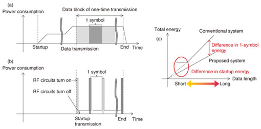
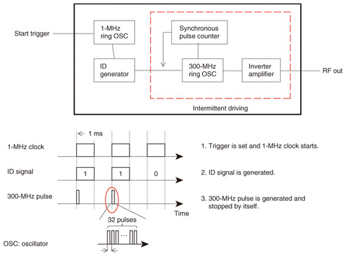
2.3 Wireless IC technology [7]In this subsection we introduce an ultralow power wireless transmitter that uses intermittent pulse train modulation. Let us start by first examining a conventional wireless system. The power consumption over time for one-time data transmission is depicted in Fig. 4(a). To transmit data, first, the wireless circuits turn on. However, some startup time is necessary before data can be transmitted. The main operations that make up the startup time are oscillator stabilization and IC reset and initialization. These operations require about 10 ms when the system uses a crystal oscillator to lock the phase-lock loop circuit. The wireless system then starts to transmit the data. During the data transmission, the power consumption consists of the power for driving the circuits and the power transmitted to the air. In theory, only the power transmitted to the air is required for wireless communications. As little power as possible should be used for oscillator stabilization and for driving the circuits.
Our wireless system is shown in Fig. 4(b). We use two key techniques to reduce the total power consumption. One is a quick startup circuit to cut off the energy loss during the stabilization time. The other is the use of a 1-symbol intermittent pulse train instead of a continuous wave, so that when the pulse stops the radio frequency (RF) circuits also stop in order to reduce the energy needed to transmit 1-symbol data. The total energy for transmitting data is shown in Fig. 4(c). When the length of the transmitting data is long, the 1-symbol energy is dominant in the total energy, and when the data length is short, the stabilization energy is dominant. The proposed system can reduce the energy used for both startup and data transmission and achieve lower energy than a conventional system. A block diagram of the proposed wireless transmitter is shown in Fig. 5. It consists of a baseband ring oscillator for a data clock, an RF ring oscillator for a pulse generator, a pulse counter, an identification (ID) generator, and a driver amplifier. The ring oscillator is effective for achieving a quick startup. When the baseband oscillator starts, the ID signals are generated. While the signal is set to 1, the RF oscillator generates a pulse train. The pulse counter counts the number of pulses and stops the RF oscillator when the count reaches 32. After that, the RF circuits stop and consume no more power. The measured power consumption of 1-bit generation is 10 nJ/bit. This means that when we transmit 50 bits of “1” data in 1 s, the total power consumption is 500 nW.
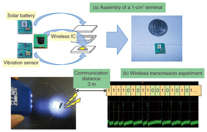
3. Fabricated WSNPhotographs of a fabricated WSN are shown in Fig. 6. The configuration is also shown. The WSN has a solar battery, vibration sensor, wireless IC, antenna, and other devices. The total volume is 1 cm3 with a small-wire dipole antenna. The 1-cm2 printed circuit boards are stacked three-dimensionally to reduce the total size. The frequency band is set to 300 MHz, which means that no usage license is necessary under low output power conditions in Japan. The data rate is 1 Mbit/s and the bandwidth is 10 MHz. The transmitted data length is 36 bits including the preamble, fixed pattern, and ID. When the WSN detects sufficient vibration, it transmits the ID. The measurement setup and results are also shown in Fig. 6. The WSN was charged with solar energy, and the data signals were then transmitted when the vibrations were detected. The ID signals were strong enough for a receiver located 3 m away to detect them and to demodulate bit data.
4. Concluding remarksThe ultrasmall WSN powered by an energy harvester is expected to lead to new services. In this article, we introduced nanowatt circuit technologies for sensing and wireless circuits. The fabricated 1-cm3 WSN successfully transmitted an ID a 3-m distance using only solar energy. In future, we will attempt to fabricate a much smaller WSN that can transmit signals a much longer distance using less energy; such an achievement would allow any object in the world to be connected to a network. References
|
||||||||||||||||