|
|||||||||||||||||||||||||||||||||||||||||||||||||
|
|
|||||||||||||||||||||||||||||||||||||||||||||||||
|
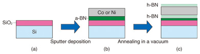
Feature Articles: Front-line Research on Graphene Vol. 11, No. 8, pp. 15–19, Aug. 2013. https://doi.org/10.53829/ntr201308fa3 A Novel and Simple Method of Growing Atomically Thin Hexagonal Boron NitrideAbstractHexagonal boron nitride (h-BN), a structural analogue of graphene, is an insulating material with a large band gap. The combination of graphene and h-BN is expected to lead to a wide variety of applications. Thus, the demand for large-area and high-quality growth of h-BN is increasing. This article describes a novel and very simple method for growing a large-area and atomically thin h-BN film. In this method, an amorphous solid source is converted to crystalline h-BN through diffusion of boron and nitrogen atoms in metal foil followed by precipitation at the surface.  1. Overview of hexagonal boron nitridePlanar materials of atomic layer thicknesses, for example, graphene, are attracting much attention for their potential use as building blocks of future nanoelectronics. Hexagonal boron nitride (h-BN) is such a layered material that has a honeycomb atomic network similar to graphene. h-BN is an insulator with a large band gap of about 6 eV [1], which is in strong contrast to graphene, which has no band gap. Various applications can be expected by combining graphene and h-BN, whose structures are similar, but whose physical properties are largely different. For example, the mobility of a graphene device is known to be largely improved when h-BN is used as a substrate compared to a conventional SiO2 substrate [2]–[5]. The reason for this is generally considered to be because h-BN has a much smaller quantity of charged impurities, which scatter carriers in graphene and reduce the mobility. Moreover, the combination of graphene and h-BN would overcome the greatest disadvantage of graphene: the poor switching property (low on/off ratio) in a FET (field-effect transistor), which originates intrinsically in the gapless electronic structure. A band gap opening is expected when graphene is transferred onto h-BN because of the stacking-induced symmetry breaking [6]–[10]. Furthermore, h-BN can also be applied as a gate insulator or a tunnel barrier in electronic devices [11], [12]. The exfoliation method has generally been used to obtain h-BN films [2], [3], [5]. In this method, a single crystal is cleaved by using adhesive tape, and a piece of the crystal is transferred onto a substrate by rubbing the tape on the substrate. (Initially, graphene was obtained exclusively using this method.) However, the typical size of the h-BN film obtained by exfoliation is only 10 mm, and the lack of scalability has prevented more common use of h-BN. Thus, the demand for large-area high-quality h-BN growth is increasing. Recently, many attempts have been made to grow large-area h-BN film by using thermal chemical vapor deposition (CVD) [4], [13]–[19]. However, the CVD method often uses a toxic and explosive gas as a feedstock. We are researching a CVD method with the objective of obtaining high-quality and controlled growth of the number of h-BN layers [19]. We have also been developing a new method of growing h-BN that would replace the CVD technique [20]. Here, we report a novel and very simple method of growing an atomically thin h-BN film, in which an amorphous material is converted to crystalline h-BN. 2. Growth of h-BN using a solid sourceOur method of growing a h-BN film is schematically shown in Fig. 1. A thermally stable SiO2/Si wafer is used as a substrate (Fig. 1(a)). An amorphous boron nitride (a-BN) film 30 nm thick is deposited on the substrate by radio frequency (rf) magnetron sputtering using a sintered BN target. Sequentially, a polycrystalline Ni or Co film 300 nm thick is deposited by rf magnetron sputtering (Fig. 1(b)). The sample was inserted in a quartz tube furnace and heated at 930°C for 10 to 30 min in a high vacuum. An atomically thin h-BN film is formed on the surface of the sample by the heating process (Fig. 1(c)). With this method, we can in principle obtain a h-BN film as large as the substrate that can be set in the furnace and sputtering machine. Another major advantage is that this method is much simpler and safer because no toxic or explosive gases are required.
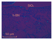
The grown h-BN film can be transferred onto any kind of substrate by etching the metal film in an acid. An optical microscope image of a h-BN film transferred to a SiO2/Si substrate is shown in Fig. 2. The h-BN film is scarcely visible because of the high transparency in the visible light. Similarly, graphene can also be transferred to a substrate. Therefore, we can fabricate various graphene/h-BN stacking structures by using the transfer technique.
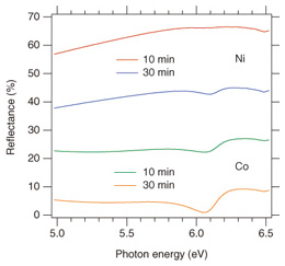
h-BN has a band gap in the ultraviolet (UV) region and reflects a part of photons whose energy is larger than the band gap. UV reflectance spectra obtained from Ni and Co samples after heating are shown in Fig. 3. The peaks observed at about 6.3 eV are characteristic in h-BN, and thus, the appearance of the peaks is indicative of the formation of h-BN (The other part of each spectrum is mainly due to reflection by a Ni or Co film underneath the h-BN film.).
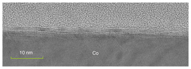
A cross-sectional transmission electron microscope image of a Co sample is shown in Fig. 4. The observed layered structure is also specific to h-BN. The figure indicates that the h-BN film consists of about four atomic layers. This growth method makes it possible to obtain such an atomically thin film.
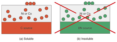
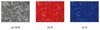
3. Growth mechanismIncidentally, why is a h-BN film formed in this method shown in Fig. 1? The B and N source material, a-BN, is initially embedded in the thick metal film. To begin with, how can B and N atoms reach the metal surface? It is known that a graphite film is formed on the surface by heating when the a-BN film in Fig. 1(b) is replaced with an amorphous carbon (a-C) film. This phenomenon is explained as follows. A considerable amount (~1 at.%) of carbon is soluble in Ni or Co at high temperatures near 1000°C, as schematically shown in Fig. 5(a). Thus, some of the carbon atoms are dissolved in the metal during the heating in the furnace. The carbon atoms dissolved at the interface move to the inside of the metal by diffusion. After a certain period, the dissolved carbon atoms are uniformly distributed in the metal. Here, heating is stopped and the temperature decreases. Accordingly, carbon solubility in the metal also decreases. Then, the excess carbon atoms, which can no longer be dissolved in the metal, precipitate on the surface and form a graphite film. One may expect that this scenario can be applied to the h-BN case. Unfortunately, however, this scenario cannot explain the h-BN formation. This is because BN or N solubility in Ni or Co is virtually zero even at high temperature. (B alone is known to be slightly soluble at high temperature.) Again, how can N atoms move in the metal and reach the surface? The detailed mechanism is not clear at present, but some experimental results have been obtained that provide some insight into the issue. A scanning electron microscope (SEM) image of a Ni sample after heating is shown in Fig. 6(a). Although the entire surface is covered by a h-BN film, it is thin enough for electrons to penetrate, and the observed contrast is due to the morphology of the Ni film. The figure shows that a polycrystalline Ni film is formed after heating, in which the typical grain size is micrometer scale. B(KLL) and N(KLL) Auger electron* mapping images showing the amount of B and N at the surface are shown in Figs. 6(b) and (c), respectively. The two images are largely correlated due to the formation of h-BN. The position-dependent intensity variation shows a thickness variation of the h-BN film. The thick (white) part often forms a closed curve along the fringe of a Ni grain. These results suggest that N atoms reach the surface by the grain boundary diffusion.
4. Future prospectsCurrently, we are trying to make this method of h-BN growth further simpler. In this study, the a-BN and metal films were deposited by the sputtering method. Recently, however, we succeeded in growing an atomically thin h-BN film using a spin-coated solid source and commercially obtained metal foil [23]. Thus, an evaporation machine is no longer necessary for growing h-BN. We are also studying the mechanism of h-BN formation. Recent experiments suggest that the diffusion of N atoms is much slower than B and that the h-BN formation is restricted by the provision of N atoms at the surface [23]. We will also try to fabricate stacking structures of h-BN and graphene with the aim of achieving high performance and high functionality graphene devices. References
|
|||||||||||||||||||||||||||||||||||||||||||||||||