|
|||||||
|
|
|||||||
|
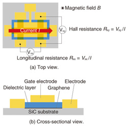
Feature Articles: Front-line Research on Graphene Vol. 11, No. 8, pp. 20–25, Aug. 2013. https://doi.org/10.53829/ntr201308fa4 Exploring Relativistic Physics and Band Gap Detection in Epitaxial GrapheneAbstractGraphene is a relatively new type of material whose charge carriers exhibit unique relativistic quantum behavior. Recent progress in graphene research has revealed that high-quality and large-scale epitaxial graphene can be obtained through thermal decomposition of SiC. This article describes electrical transport measurements of carrier-density-tunable epitaxial graphene devices that shed new light on graphene. For epitaxial monolayer graphene, we first report on the unusual quantum Hall effect derived from the relativistic nature of the charge carriers and further elucidate its associated physical features. For epitaxial bilayer graphene, we present a signature of a band-gap opening that can be induced by the field effect.  1. IntroductionGraphene is a two-dimensional honeycomb lattice of carbon atoms. It was first mentioned by Dr. P. R. Wallace in the 1940s as a fascinating but imaginary concept. He found that charge carriers in graphene were governed by the relativistic quantum theory instead of by the usual quantum mechanics or classical mechanics that normally describes the motions of carriers in a solid. However, it was presumed that graphene did not exist in the real world because researchers thought that it went against the Mermin–Wagner theorem stating that a macroscopic crystalline order does not exist in two-dimensional systems at finite temperatures. This consensus on graphene was broken in 2004 and 2005 with the report stating that a monolayer of graphite, i.e., graphene, exfoliated from bulk graphite on SiO2/Si, shows transport features of massless Dirac fermions, which are derived from the relativistic theory. Shortly after these reports were published, the stability of graphene was found to be compatible with the Mermin–Wagner theorem due to its corrugation structures, and the remarkable discovery of graphene sparked research in a variety of fields. This is because graphene is more than just a new material; it opens up possibilities for table-top experiments demonstrating relativistic physics, which have conventionally been investigated using large accelerators. This breakthrough was so remarkable that it resulted in the 2010 Nobel Prize in Physics being awarded to the researchers only five to six years after their discovery. However, studies on graphene still have a long way to go. It is likely that such studies will be extended to even more diverse fields and will also face various problems. One important issue that should be addressed is the need to develop a means of growing high-quality and large-area graphene that is suitable for industrial applications. In this article, we present our recent research on the transport properties of monolayer and bilayer graphene grown on SiC, which we hereafter refer to as epitaxial monolayer graphene and epitaxial bilayer graphene, respectively. We first show that devices fabricated from epitaxial monolayer graphene have a high level of quality that is comparable to those fabricated using the standard exfoliation technique. This is demonstrated by the observation of a robust half-integer quantum Hall effect, which is a hallmark of the relativistic nature of charge carriers [1]. Then we show that transport measurements of epitaxial monolayer graphene can also be used as a form of energy spectroscopy of graphene [2]. Unlike monolayer graphene, bilayer graphene is predicted to have a band gap, which has previously been investigated by optical measurements. We report here that transport measurements of epitaxial bilayer graphene can detect the signature of the band gap [3]. 2. Experimental methodsWe obtained epitaxial monolayer graphene and epitaxial bilayer graphene through thermal decomposition of SiC(0001). By choosing the appropriate growth conditions, we can preferentially grow either a monolayer or bilayer of graphene on a wafer scale in a controlled manner. We fabricated top-gated Hall bar devices using these graphene layers as the channel. Schematics of the top and cross-sectional views of the devices used in this study are shown in Figs. 1(a) and (b). A gate electrode was formed above the graphene channel, separated by a dielectric layer. Applying a gate voltage between the graphene channel and the gate electrode allows us to tune the carrier density over a wide range across the charge neutrality point. Transport measurements were performed at temperatures ranging between ~1.5 and 300 K. Magnetic fields of up to 10 T were applied perpendicular to the graphene sheet for Hall measurements (Fig. 1(a)). These experimental conditions are sufficient to study the physics discussed in this article.
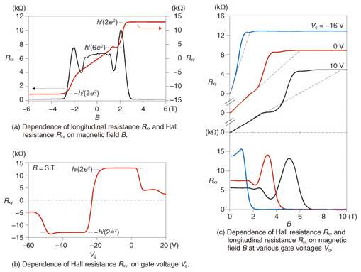
3. Monolayer graphene: half-integer quantum Hall effectHere, we describe the results of transport measurements of an epitaxial-monolayer graphene device, obtained at a temperature of 1.5 K and in fields from 0 to 10 T. The Hall resistance (red line) and longitudinal resistance (black line) as a function of magnetic field, obtained with gate voltage Vg fixed at zero are shown in Fig. 2(a). At low fields, the Hall resistance increases proportionally with the field, while at high fields a region referred to as a plateau appears, which is characterized by a constant Hall resistance accompanied by zero longitudinal resistance. This is a phenomenon universally observed in two-dimensional electron or hole systems induced at high-quality semiconductor interfaces, and is a consequence of the discrete energy levels referred to as Landau levels that form at high fields. If we consider for simplicity spin-split Landau levels, then charge carriers filled in one Landau level contribute to Hall conductance by e2/h. Accordingly, the Hall resistance is quantized to h/ie2 with i being an integer, the phenomenon known as the integer quantum Hall effect (QHE). For the QHE in monolayer graphene, the Hall resistance is predicted to take the values h/{4(N+1/2)e2} (N: integer) at the plateaus. Because graphene has a fourfold degeneracy due to spin and valley degrees of freedom, the integer in the denominator changes by 4N. Interestingly, a unique feature arises at the first (N = 0) plateau. The resistance becomes h/{4×(0+ 1/2)e2}=h/(2e2), and thus, a half-integer shift seems to occur. This shift is a consequence of the relativistic energy spectrum, because at high fields graphene has a zero-energy state arising from the coexistence of electrons and holes, which are equally responsible for the fourfold degeneracy.
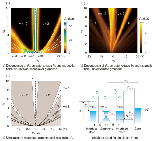
In Fig. 2(a), plateaus labeled by the resistance values of ±h/(2e2) and h/(6e2) are observed, and at the same time, longitudinal resistance becomes zero at the ±h/(2e2) plateaus. We can thus say that the ν = 2 quantum Hall effect (ν : the filling factor, i.e., the number of Landau levels filled with electrons or holes) is well developed. Furthermore, we can also confirm that graphene has bipolar charged carriers by observing the dependence of Hall resistance on Vg (Fig. 2(b)), which changes from positive to negative at Vg = −22 V because of changes in the positive and negative signs of the carriers. These observations in which we verified the bipolar half-integer quantum Hall effect led to the conclusion that our device fabricated from epitaxial monolayer graphene is as high in quality as those fabricated from graphene exfoliated from bulk graphite [1]. Moreover, in our devices, the carrier density can be modulated over a wide range using the gate electrode. Then the type of carrier can be varied between electrons and holes across the Dirac point, where electrons and holes ideally vanish. Such a device using epitaxial monolayer graphene has not been demonstrated previously. This gives us a definite advantage in exploring an area of physics that has not been revealed for epitaxial monolayer graphene. 4. Monolayer graphene: spectroscopy through transport measurementsNext, we show an example to illustrate the advantage of the wide tunability offered by our epitaxial- monolayer graphene devices. The results were measured for another sample and show the field-dependence of Hall and longitudinal resistances obtained for different gate voltages; these results are shown in Fig. 2(c). As the graph clearly shows, the ν = 2 QH regime starts from lower fields for lower carrier densities, and it persists up to the highest field for all the carrier densities shown. This feature has not been observed for graphene on SiO2/Si, and is thus a feature specific to epitaxial monolayer graphene, referred to as the anomalously wide ν = 2 QH state. The mechanism for this anomalous behavior has remained elusive but was recently revealed by our study, as reported below. A mapping of longitudinal resistance Rxx plotted as a function of gate voltage and magnetic field is shown in Fig. 3(a). The trajectories of Rxx peaks displayed in Fig. 2(c) are represented in Fig. 3(a) as parabolic curves centered at Vg = −37 V. Rxx mapping obtained for a conventional exfoliated graphene device shows linear trajectories of the Rxx peaks, as presented in Fig. 3(b). A comparison of Figs. 3(a) and (b) demonstrates that the ν = 2 QH regime is significantly wider in epitaxial monolayer graphene than in exfoliated graphene. This anomalous wideness is intuitively attributed firstly to the parabolic trajectories of the Rxx peaks and secondly to the width of the Rxx peak at ν = 0, which is nearly unchanged with increasing fields.
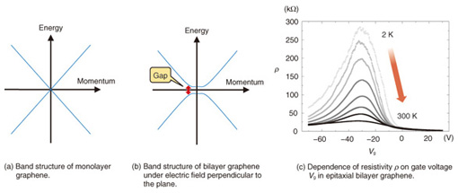
To clarify the underlying mechanism of the anomalously wide ν = 2 QH regime, we first examined the Vg dependence of the carrier density deduced from Hall resistance at low fields. The Vg dependence would be linear in ideal two-dimensional systems; however, it is parabolic in our epitaxial-monolayer graphene devices. In addition, around the Dirac point, the change in carrier density induced by a change in Vg is much smaller than that expected from the device geometry. This may indicate that some additional charge reservoir other than graphene exists in the devices. Likely candidates are interface states such as dangling-bond states at the interface with the SiC substrate or those in the gate insulator; the former is known to inevitably occur in devices fabricated from epitaxial monolayer graphene grown under standard conditions. We then developed a model describing the interplay between graphene quantum capacitance and interface-state capacitances (Fig. 3(d)). By applying this model to the Vg dependence of the carrier density deduced at low fields, we can deduce the interface state densities and reproduce the trajectories of the Rxx peaks in the gate-voltage vs. field plane (Fig. 3(a), white dashed lines). Furthermore, when we take into account the fourfold degeneracy of graphene Landau levels, we can calculate the borderlines separating integer and noninteger ν, which are in good agreement with our experiment. Therefore, our study demonstrates that the origin of the anomalously wide ν = 2 QH state is the interplay between graphene quantum capacitance and interface-state capacitances [2]. More importantly, when the interface state densities are much larger than the density of states in graphene, the Fermi energy of graphene becomes proportional to the gate voltage. Consequently, the Rxx peaks plotted vs. Vg and field closely resemble the relativistic LL (Landau level) diagram plotted vs. energy and field. This indicates that transport measurements serve as a kind of spectroscopy, which allows us to deduce the energy width of the disorder-broadened LLs, which has been an important issue in graphene research. 5. Bilayer graphene: electrical detection of band gap openingWe next present a signature of a band gap opening in epitaxial bilayer graphene. In order to explain our experimental results, we briefly describe the band structures of monolayer graphene and bilayer graphene. The energy band structure of monolayer graphene is shown in Fig. 4(a). The conduction and valence bands touch each other at the Dirac point, which means that monolayer graphene does not have a band gap. This becomes a drawback of monolayer graphene when it is used as a channel in logic devices because a large on/off ratio cannot be expected. Although graphene that is patterned into nanoribbons, which are strips of graphene in nanometer-scale width, is predicted to have a band gap, making such nanoribbons with uniform widths and controlled edge structures is still a formidable experimental challenge.
However, opening a band gap was more easily achieved in bilayer graphene, where a band gap appears between the valence and conduction bands when there is a potential difference between the two graphene layers, as shown in Fig. 4(b). The potential difference can be easily induced by applying an electric field perpendicular to the two graphene planes in a gated structure, as shown in Fig. 1. Thus, opening a band gap is more feasible in bilayer graphene than in monolayer graphene. Our experimental results on the gate-voltage dependences of resistivity of a top-gated Hall bar device using epitaxial bilayer graphene are shown in Fig. 4(c). The data at 2 K indicate that when the gate voltage is reduced from 0 to −30 V, the resistivity increases and reaches a maximum at −30 V. The resistivity decreases as the gate voltage is further reduced from −30 to −70 V. In a Hall effect measurement, the polarity of the Hall voltage indicates that from 0 to −30 V the carriers are electrons, and their density decreases as the gate voltage approaches −30 V. The polarity of the Hall voltage is reversed when the gate voltage is reduced from −30 to −70 V, which indicates that carriers are holes in this gate voltage range. Also, the hole density increases as the gate voltage approaches −70 V. These results indicate that the increase in resistivity is due to the decrease in carrier density. It is also clear from Fig. 4(c) that the value of the maximum resistivity decreases with increasing temperature. The strong temperature dependence of the maximum resistivity indicates that epitaxial bilayer graphene exhibits insulating behavior. This is compatible with the theoretical prediction that a band gap can be opened by the applied field effect, since the observed features can be understood by the scenario where the carriers are thermally excited from the Fermi level situated in the gap to the conduction or valence bands. Therefore, we can conclude that we have observed a signature of the band gap opening in epitaxial bilayer graphene. Such a band gap can be tuned by the field effect and scalability of the graphene growth to an arbitrary size, which makes epitaxial bilayer graphene a very promising material for use as channels in integrated transistors. 6. Summary and future prospectsWe have reported our recent experimental results on charge transport in monolayer and bilayer graphene grown on SiC. We demonstrated that epitaxial monolayer graphene shows significant relativistic charge transport and that our field-effect gated device is useful for further study of unique graphene physics. We found that for epitaxial bilayer graphene, a band gap could be opened because of the applied field effect, which will enable future applications as channels of electronic devices. References
|
|||||||