|
|||||||||
|
|
|||||||||
       |
Feature Articles: Cutting-edge Device and Materials Technologies for Creating New Business Vol. 12, No. 4, pp. 51–56, Apr. 2014. https://doi.org/10.53829/ntr201404fa8 GaN-on-Si Technology for High-power TransistorsAbstractGroup-III nitride semiconductors are very promising materials for high-power electronic devices. The physical properties of these semiconductors make it possible to develop devices that show better performance than the silicon (Si)-based devices that are currently used for integrated circuits. In particular, replacing Si-based devices in inverters, which are widely used in home appliances, with gallium nitride (GaN)-based devices is an effective way to reduce electric power consumption in homes. In this article, a technique for forming GaN and related materials on Si substrates is introduced. This technique is suitable for low-cost mass production techniques because Si substrates have the largest size and lowest cost among various substrates. Keywords: GaN, Si substrate, epitaxial growth
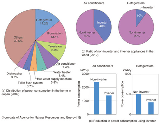
1. Overview of nitride semiconductorsNitride semiconductors are a type of compound semiconductor that are composed of a group-III element and nitrogen, for example, gallium nitride (GaN), aluminum nitride (AlN), indium nitride (InN), or a combination of these materials. These semiconductors have a band gap corresponding to short-wavelength light, and they are chemically and mechanically very stable. This gives them high potential strength even in high-temperature environments. Recently, light-emitting diodes (LEDs) have come to be widely used as lighting devices in place of incandescent light bulbs or fluorescent lamps. These LEDs are made with nitride semiconductors. Nitride semiconductors are thus widely used in many familiar applications. 2. Promising applications of nitride semiconductorsThe use of LEDs made of nitride semiconductors can contribute to reducing electric power consumption, and this is one reason why nitride semiconductors are promising materials. Another large energy-saving effect is achieved when nitride semiconductors are applied to devices used in power supply units in home appliances. One such example is the circuit that drives the motor in compressors used in refrigerators and air conditioners. In Japan, a circuit called an inverter is used in most home appliances. The inverter generates an AC (alternating current) signal with an arbitrary frequency by using the switching function of transistors, and it can control the amount of electric power that is supplied by changing the frequency. The power consumption of the inverter is much lower than that of the power unit that controls the supplied power by simply switching the electric power on and off. As described above, most refrigerators and air conditioners in Japan already have power units that include an inverter. However, the use of inverters is not as widespread in other developed and developing countries. An extremely large reduction in power consumption around the world could be achieved by replacing non-inverter products with inverter ones (Fig. 1). The power-saving effect from replacing all non-inverter type power units in refrigerators and air conditioners throughout the world with inverter ones is estimated to equal the amount of electric power produced by eight thermal power plants [1]. Moreover, the use of GaN-based transistors instead of silicon (Si)-based transistors, which are included in inverters, is estimated to result in a one-third to one-half reduction in power consumption. Therefore, GaN-based transistors are considered to be very promising devices for saving power.
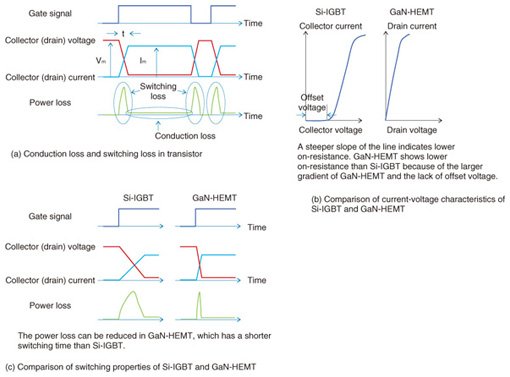
3. Mechanism of achieving low power consumption with GaN-based transistorsI discuss here the mechanism in which power consumption can be reduced using GaN-based transistors [2]. There are two main factors in the power loss that occurs because of the characteristics of transistors in the inverter circuit. One is the conduction loss, which corresponds to the power loss when current is flowing through transistors. Conduction losses increase as the on-resistance increases. This refers to the resistance of the current path between terminals when the transistor is in the on-state. The other factor is the switching loss that occurs when transistors are switched from the on-state (in which current flows through transistors) to the off-state (in which current does not flow) and vice versa (as shown in Fig. 2(a)). These are described in more detail in the following subsections. 3.1 Conduction lossSi-based devices called insulated gate bipolar transistors (IGBTs) are typically used in the inverter circuit. The IGBT has three terminals consisting of a gate, emitter, and collector. Current flows from the collector to the emitter; we can switch the IGBT from the on-state to the off-state by applying bias voltage to the gate. The electron density in the area where current flows in the IGBT is relatively low in order to avoid breakdown during high-voltage operation. This is one reason why the on-resistance of IGBTs is large. Moreover, no current flows below a certain voltage (called offset voltage) between the emitter and collector because of this operating principle. This is another reason for the large on-resistance in IGBTs. In turn, transistors called high-electron mobility transistors (HEMTs) are widely used in GaN-based transistors. The HEMT has a channel layer with a very high density of electrons, which is known as two-dimensional electron gas (2DEG). The electron mobility of 2DEG is very high, as the device name suggests. HEMTs also have three terminals consisting of a gate, source, and drain. Current flows from the drain to the source, and we can switch the HEMT from the on-state to the off-state by applying bias voltage to the gate in the same manner as the IGBT. Consequently, because nitride-based semiconductors have higher breakdown strength than Si, a GaN-based HEMT can be operated under higher voltage. In addition, the HEMT has essentially no offset voltage (Fig. 2(b)). Therefore, GaN-based HEMTs have much smaller on-resistance than Si-based IGBTs. As a result, using GaN-based HEMTs instead of IGBTs can reduce the conductive power loss to half or less.
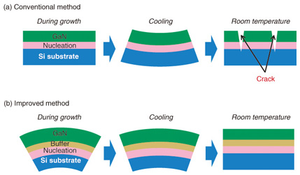
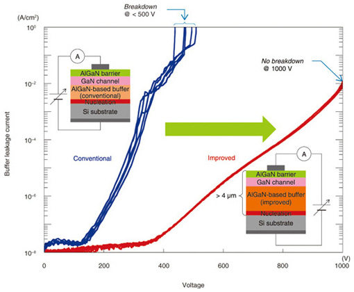
3.2 Switching lossIn the inverter circuit, transistors are switched from the on-state to the off-state, or vice versa, by changing the gate bias voltage. In the on-state, the current flowing from the collector to the emitter (IGBT) or from the drain to the source (HEMT) shows the maximum value (Im) when the voltage between the collector and emitter or the drain and source is very small (limited by the on-resistance). On the contrary, in the off-state, a certain voltage (Vm) between the collector and emitter or the drain and source is applied while the current from the collector to the emitter or from the drain to the source is almost zero. Therefore, the power loss per unit time in the on- or off-state itself is very small. The power loss during the switching between the on-state and the off-state is called the switching loss. Power consumption in transistors is approximately given by the product of the current, voltage, and duration time. If the switching from the on- to off-state or from the off- to on-state is fast enough, the switching loss is negligible. However, the switching time in actual devices is not zero but a finite value. As a result, switching loss occurs. The switching loss can be reduced by shortening the switching time. The operating speed of GaN-based HEMTs is much higher (about 10 times higher) than Si-based IGBTs. Therefore, the switching loss can be reduced by replacing Si-based IGBTs with GaN-based HEMTs. 4. Low-cost GaN-based HEMTs using GaN-on-Si technologyWith Si-based transistors, devices are fabricated directly on Si substrates using various process technologies such as thin film deposition, impurity diffusion, ion implantation, or electrode formation. On the contrary, in the case of GaN-based transistors, the transistors cannot be fabricated until nitride semiconductor films are first formed on the substrate using an epitaxial growth technique. This section focuses on the epitaxial growth of GaN-based materials. 4.1 Growth of semiconductor materials on substratesThe first process in fabricating III-V compound semiconductors, including nitride semiconductors, is the epitaxial growth of semiconductor materials on substrates. There are various methods of growing semiconductor materials; the vapor phase epitaxial technique is one widely used method. Substrates made of the same material or made with other materials that have similar properties are commonly used for epitaxial growth because high quality semiconductors can be obtained using such substrates. However, substrates consisting of nitride semiconductors are currently very expensive, and their size is rather small because of the difficulty in producing nitride substrates. Because GaN-based HEMTs are used in home appliances, it is essential to achieve cost competitiveness. In view of this, GaN-on-Si technology, by which nitride semiconductor materials are grown on Si substrates, has attracted a lot of attention. That is, nitride semiconductors are grown on a large scale on high-quality and low-cost Si substrates that are easily obtained. 4.2 Technical problems related to growth of materialsMany technical problems first need to be solved, however, in order to successfully grow GaN-based materials on Si substrates. The most serious issue to be solved is the mismatch in material properties between GaN and Si. The process of growing semiconductors is greatly affected by the properties of substrates. One of the most important properties is the lattice constant, which is the unit size of the crystal structure of the material. Individual materials have different lattice constants. The mismatch in the lattice constant between a substrate and a material grown on the substrate should generally be less than 0.1%. However, the lattice mismatch between GaN and Si is over 14%. Therefore, we have to overcome a lattice mismatch that is 100 times larger in order to develop effective GaN-on-Si technology. Another important property is the thermal expansion coefficient. The lattice of the material expands and shrinks as the temperature increases and decreases. The thermal expansion coefficient is defined as the ratio between the change in the lattice constant due to a temperature change of 1 K and the lattice constant itself. The growth temperature of GaN and related materials is very high at about 1000°C. When the substrate is cooled down to room temperature after growth, both the GaN layer and the Si substrate shrink. Because GaN has a larger thermal expansion coefficient than Si, the Si substrate with the GaN layer has a concave shape. If the curvature of the substrate exceeds the limit of the mechanical strength of the material, the GaN layer will crack over the entire substrate (Fig. 3(a)). Therefore, it is also necessary to overcome the mismatch in the thermal expansion coefficient between GaN and Si. A buffer layer that can compensate for the mismatch between material properties such as the lattice constant and the thermal expansion coefficient is usually grown between the Si substrate and the GaN layer. At NTT Photonics Laboratories, we have been investigating the structure of the buffer layer and have successfully obtained high quality GaN-based HEMT structures on Si substrates [3] (Fig. 3(b)). We are now planning to develop GaN-on-Si technology that is even more cost-effective. Until now, we have been able to successfully grow GaN-based HEMT structures more than 4 µm thick on large Si substrates up to 6 inches in diameter by using an improved buffer structure. This has resulted in electrically robust properties in which the fabricated structure does not crack even if subjected to very high voltage exceeding 1000 V (Fig. 4). The GaN-based HEMTs fabricated using GaN-on-Si technology are expected to be widely used in green devices that will contribute to achieving an energy-saving society in the near future.
5. ConclusionThis article described a technique for forming GaN and related materials on Si substrates. This technique is suitable for low-cost mass production because substrates fabricated from Si are the largest in size and lowest in cost among various substrates. However, some issues remain to be solved. One of the most serious issues is current collapse, a phenomenon in which the on-resistance of a transistor gradually increases during transistor operation. These issues are now under investigation. Nevertheless, the GaN-on-Si technology is expected to lead to the development of devices that are indispensable for an energy-saving society. References
|
||||||||