|
|||||||||||||||||||||||||||||||||||||
|
|
|||||||||||||||||||||||||||||||||||||
|
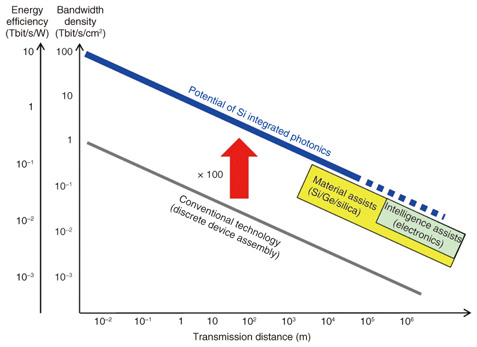
Regular Articles Vol. 12, No. 5, pp. 42–51, May 2014. https://doi.org/10.53829/ntr201405ra1 Silicon-germanium-silica Monolithic Photonic Integration Platform for Telecommunications Device ApplicationsAbstractWe have developed a silicon (Si)-germanium (Ge)-silica monolithic photonic integration platform for telecommunications applications of highly integrated silicon-based photonic devices. On this platform, high-performance silica-based passive devices and compact, high-speed Si/Ge-based active devices are monolithically integrated. We have used this platform to develop a photonic receiver for wavelength- division multiplexing systems, in which a silica-based 16-channel arrayed waveguide grating wavelength filter and Ge photodiodes are monolithically integrated. This Si-Ge-silica photonic integration platform also enables direct integration of electronic circuits. Keywords: silicon photonics, integrated photonic circuit, photonics electronics convergence  1. IntroductionTelecommunications network systems are now facing an explosive traffic increase with a growth rate of 30% per year [1]. However, such large and rapid growth is not sustainable from economic and environmental viewpoints because within ten years, the energy consumption and capital/operating expenditure for network systems would increase by ten times or more. One of the breakthrough technologies for dealing with this information explosion is high-density photonic integration with ultra-small photonic devices. The smaller the device is, the less power is required. Moreover, integrated photonic functions with redundancy enable flexible and energy-efficient network operation [2]. Silicon photonics, one of the most promising technologies for such high-density photonic integration, enables monolithic integration of photonic devices made of silicon (Si) and germanium (Ge) on a Si wafer. In particular, Si photonic wire waveguides with a micrometer-scale bending radius and a sub-micrometer-scale core enable ultrahigh density photonic device integration [3]. The potential of silicon photonics technology in data transmission systems is shown in Fig. 1. The compactness of the silicon photonic devices could lead to a 100-fold improvement in both energy efficiency and integration density, compared to those in conventional technology. Although the improvement could be implemented in a wide area of applications ranging from on-chip interconnects to long-distance telecommunications, the hurdles to telecommunications applications are still very high. In telecommunications applications, where long-distance optical transmission is essential, devices should have low optical losses, low interchannel crosstalk, and insensitivity to polarization. For example, in dense wavelength-division multiplexing (WDM) transmission systems, interchannel crosstalk should be less than –25 dB. The present Si photonic platform, however, cannot provide such high-performance photonic devices. In particular, the performance of passive photonic devices, for example, wavelength filters, is a critical issue. Several wavelength filters based on Si photonic wire waveguides have been reported [4], [5], but none of them meet the requirements for telecommunications applications. The effective refractive index of a Si photonic wire waveguide is extremely sensitive to the core geometry, and therefore, the geometric tolerance required is far below that of the errors in the present fabrication technology. For example, a 1-nm geometric error significantly increases the interchannel crosstalk of a wavelength filter to –18 dB, which is not acceptable for telecommunications applications [6].
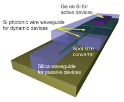
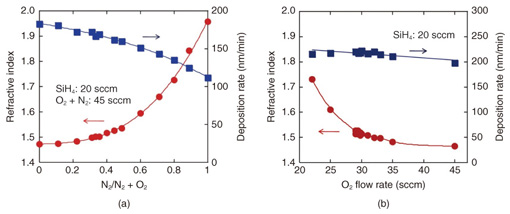
To eliminate these obstacles to practical telecommunications applications, some assisting technologies should be implemented in Si photonics. These technologies are known as intelligence assists and material assists, as shown in Fig. 1. Intelligence assists are aimed at compensating for performance deficiencies by using digital electronics, which are now being developed in digital coherent transmission systems. Material assists are designed to improve performance by introducing the right materials for the right functions. One of the most promising material-assist technologies is Si-Ge-silica photonic integration, which can potentially relax the geometric tolerance in high-performance passive devices. We recently developed such a Si-Ge-silica photonic integration technology, by which high-performance silica-based passive devices and Si/Ge-based compact active/dynamic devices can be monolithically integrated. In this article, we report the details of the Si-Ge-silica monolithic integration platform and its application to receivers for telecommunications systems. 2. Si-Ge-silica monolithic photonic integration platform2.1 Waveguide systemA schematic image of the Si-Ge-silica monolithic integration platform is shown in Fig. 2. This platform consists of Si-waveguide-based dynamic/active devices such as Si modulators and Ge detectors, silica-waveguide-based high-performance passive devices such as wavelength filters, and inverse-taper spot size converters (SSCs), which connect the Si and silica waveguides to each other [7]. These devices are monolithically fabricated on a silicon-on-insulator (SOI) wafer. Integration of Si- and Ge-based devices is possible using conventional Si photonics technology. However, additional silica-based devices cannot be integrated using conventional technology because conventional silica waveguide fabrication generally involves processes with temperatures exceeding 1000ºC for silica film deposition [8]. Such high-temperature processes can destroy the Si/Ge electronic structures for modulators and detectors. Our monolithic integration process features low-temperature silica film deposition using the electron-cyclotron-resonance plasma-enhanced chemical vapor deposition method (ECR-PECVD) [9]. ECR-PECVD involves the deposition of silica-based materials such as silicon oxinitride (SiOxNy) and silicon-rich silica (SiOx). A gas mixture of oxygen (O2), nitrogen (N2), and silane (SiH4) is used for the SiOxNy, and O2 and SiH4 are used for the SiOx deposition. The O2 and N2 gases are introduced into the plasma chamber, and the SiH4 gas is introduced into the deposition chamber. ECR plasma generated in the plasma chamber is transported to the deposition chamber by a divergent magnetic field and irradiated to a wafer in the deposition chamber. The energy of the ions irradiated to the wafer is about 10–20 eV [10]. This moderate energy induces a reaction on the wafer surface so that high-quality films are formed at low temperature. The ECR-PECVD system does not add bias to the substrate, so the wafer temperature during the film deposition can be kept below 200ºC even without wafer cooling. The refractive index of the deposited films is controlled by adjusting the flow rate of O2 and N2 for SiOxNy films and the flow rate of O2 for SiOx films while maintaining the flow of SiH4 at a fixed rate. The refractive index and deposition rate as a function of gas flow rate are shown in Fig. 3. Index controllable ranges are 1.47–1.72 for SiOx and 1.47–1.95 for SiOxNy. The deposition rate is over 100 nm/min. The atomic percentages were measured by Rutherford backscattering spectrometry, and we confirmed that the composition of the thermal-oxide film (reference) was precisely measured to be SiO2.0 with this technique. The compositions of the SiOx and SiOxNy cores with a refractive index contrast Δ (delta) of 2.9%, and of the clad films were SiO1.7, SiO1.8N0.2, and SiO2.0, respectively. These results indicate that the refractive indices of the silica-based films can be successfully controlled by the atomic ratio of Si/O (N). Here, for the WDM devices, the SiOx core was used for most of the passive devices because it has lower optical absorption in the C-band than the SiOxNy core.
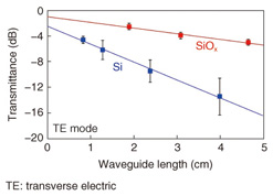
Transmission characteristics of monolithically integrated Si and SiOx waveguides with a delta of 2.9% are shown in Fig. 4. The core size of the Si and SiOx waveguides are 200 nm × 400 nm and 3 μm × 3 μm, respectively. In the sample preparation, we fabricated the Si waveguide core using electron beam lithography and low-pressure-plasma reactive ion etching before constructing the SiOx waveguides. The propagation losses of the Si and SiOx waveguides on the Si/Ge/silica monolithic platform were less than 3 dB/cm and 0.9 dB/cm, respectively. Without Ge, these losses can be further reduced to 1 dB/cm and 0.2 dB/cm, respectively. The polarization-dependent propagation loss of the SiOx waveguides is less than 0.1 dB/cm [11].
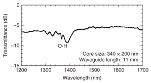
The SiOx waveguide and Si waveguide can be connected by an SSC using an inverse adiabatic Si waveguide taper. The taper tip of the SSCs is 200 nm × 80 nm, which provides a reflection ratio in the taper region of less than –40 dB [12]. The typical coupling loss per SSC is 0.35 dB for TE (transverse electric)-like modes and 0.31 dB for TM (transverse-magnetic)-like modes, respectively [13]. These coupling losses are low enough to meet the severe telecommunications-grade requirements of the platform. The transmission spectrum of a Si photonic wire waveguide with an SSC is shown in Fig. 5. Although there is absorption due to oxygen-hydrogen (O-H) residue in the SiOx film, the applicable bandwidth of the SSC is very wide, ranging from 1400 to 1700 nm for 1-dB loss. The O-H absorption can easily be eliminated by thermal annealing, and the applicable bandwidth can be further expanded.
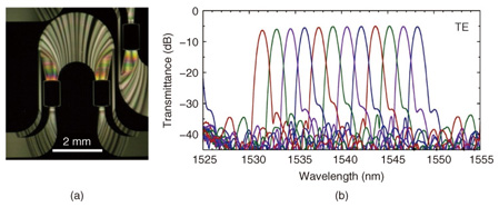
2.2 Stand-alone devicesWe used the SiOx waveguides to develope a 12-channel arrayed waveguide grating (AWG) wavelength filter with 1.6-nm channel separation. The structure and filtering spectra of the device are shown in Fig. 6. The fiber-to-fiber insertion loss is 5 dB and interchannel crosstalk is less than –25 dB. Thanks to a large waveguide core and moderate index contrast, the filtering performance is better than that in Si-based AWGs. The insertion loss and crosstalk would be further improved by applying sophisticated designs developed for conventional silica waveguide devices. Although small polarization dependence due to film stress remains in the SiOx AWG, we can compensate for it by introducing a multilayer core technology using SiOx and silicon nitride films [11].
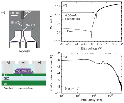
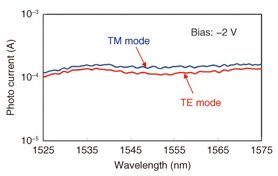
We also constructed Ge photodetectors on our Si-Ge-silica photonic platform. The structure of a Ge-based photodiode (Ge PD) with a Si waveguide input is shown in Fig. 7(a) [13]. The fabrication process for the Ge PD on the Si/Ge/silica platform is much more complicated than that of modulation devices. First, Si waveguide cores and tapers for SSCs are fabricated on the SOI wafer, and boron implantation for p-type electrodes is performed. Next, selective growth of Ge is carried out by using the UHV-CVD (ultrahigh vacuum chemical vapor deposition) method [14], and a thin Si film is deposited on the Ge surface to prevent the Ge film from being damaged during subsequent processes. After that, phosphine is implanted into the top of the Ge PD, followed by the formation of Ti/TiN/Al electrodes. Then, SiOx film is deposited by using ECR-PECVD, which is then etched to form cores of SiOx waveguides. Finally, an over-cladding SiO2 film is deposited, and contact-holes are formed. The current-voltage curves of a Ge PD in the dark and in an illuminated state are shown in Fig. 7(b). Input light power was 0.36 mW at the SSC before the Ge PD. Dark current and photocurrent were 56 nA and 0.4 mA at a –1-V bias. The responsivity of the stand-alone Ge PD was estimated to be about 1.1 A/W at the entrance of the SSC. The series resistance of the Ge PD was estimated to be about 140 Ω. The low parasitic resistance makes it possible to reduce RC (resistance capacitance) delay and improves the operation speed of the PD. The frequency response of the Ge PD is shown in Fig. 7(c). The 3-dB cutoff frequency is about 20 GHz at a –1-V bias, which would be fast enough for application to 25-Gbit/s data transmission. The relationship between photocurrent and wavelength is shown in Fig. 8 [13]. The Ge PDs show a flat wavelength dependence in the C-band, and the polarization dependence of the power amplitude is less than 1.0 dB.
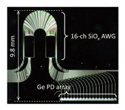
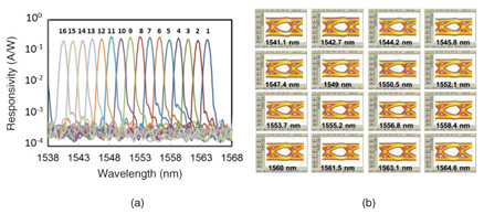
For modulation devices, we developed a polarization-independent Si-based variable optical attenuator with a p-i-n carrier injection structure [15] and Si-based p-n depletion-type optical modulators with a 10-Gbit/s modulation speed. 3. Photonic integration for WDM receiversFor WDM receiver applications, we integrated Ge PDs and an AWG on our Si-Ge-silica photonic platform. The structure of the device is shown in Fig. 9 [13]. The basic structure of the AWG is the same as that of the stand-alone device, except for the number of channels and the polarization treatment. We adopted a 16-ch AWG in this integration to use in a feasibility study of a 400-Gbit/s WDM receiver system. A slight polarization-dependent wavelength shift (PDλ) of approximately 2.0 nm remained in this AWG because we used a single-layer SiOx core to ascertain the feasibility of the integration process. The Ge PD was the same as that described in the previous section. At each output of the AWG, Ge PDs were connected via SSCs. Measured demultiplexing (DEMUX) spectra for all 16 channels of the Ge PDs are shown in Fig. 10(a) [13]. The spectra show a channel spacing of 1.6 nm as designed, and interchannel crosstalk is around –22 dB or less. The insertion loss of the AWG at the central wavelength is about 5.1 dB, which includes waveguide propagation loss of 1.8 dB and diffraction loss of 3.3 dB. The fiber-to-waveguide coupling loss is 0.48 dB/facet. The fiber-to-PD responsivity, which is normalized at the input power before the AWG, is 0.29 A/W at the central wavelength. The monolithic integration of the high-performance SiOx AWG with Ge PDs contributes to reducing crosstalk and increasing responsivity compared to a Si AWG with Ge PDs [16] and a SiN AWG with Ge PDs [17].
Next, we input non-return-to-zero (NRZ) pseudo-random bit sequence (PRBS) data with a pattern length of 231-1 into the AWG. Measured eye diagrams of DEMUX photocurrent with 22-Gbit/s signal inputs for all channels are shown in Fig. 10(b) [13]. We confirmed that all 16 channels show clear eye openings. The AWG-PD chip achieved a total system bandwidth of 352 Gbit/s. Here, the bit rate was limited to 22 Gbit/s by the measurement equipment. Since the Ge PDs can work at 25 Gbit/s as mentioned in the previous section, the total system bandwidth could potentially reach 400 Gbit/s.
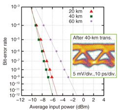
We also examined long-distance transmission in order to confirm the feasibility of the device for practical network applications. Continuous-wave infrared light from a tunable laser diode was modulated by a lithium-niobate Mach-Zehnder modulator. The modulation format was simple intensity modulation with 12.5-Gbit/s NRZ PRBS data. The word length here was also 231-1. The signal bandwidth was restricted to 12.5 Gbit/s by our experimental equipment. The modulated optical signal was transmitted through standard single-mode fibers with dispersion of 17 ps/km/nm at distances of 20, 40, and 60 km. After the polarization was prepared, the signal was input into the AWG-PD device by butt coupling of a high-NA (numerical aperture) fiber. The experiment was performed at room temperature without temperature control. The electrical signals from Ge PDs were directly guided to an oscilloscope or an error detector for bit-error rate (BER) measurement without transimpedance amplifiers (TIAs). We used a commercial clock-data recovery (CDR) module to emulate a real receiver. The input light was tapped by a 10-dB coupler and guided into the CDR module. The measured BER curves obtained from channel 12 for various transmission distances, and a received eye diagram after 40-km transmission (inset), are shown in Fig. 11 [13]. The channel numbers are shown in Fig. 10(a). We confirmed error-free signal transmission up to 40 km. The receiver sensitivity measured at the AWG input was –6.8 dBm for the BER of 10−9 after 40-km transmission. After 60-km transmission, the BER increased considerably because of waveform distortion due to the dispersion and nonlinearity of the fiber. We estimated the sensitivity of the Ge PD on channel 12 to be –13.6 dBm for the 40-km transmission, which takes into account the transmission loss of the AWG. Although the theoretical sensitivity of the AWG-PD device was –32 dBm, which was estimated from shot noise and Johnson noise [18], the measured sensitivity was restricted by the measurement system in that there were no TIAs on this chip. We believe the sensitivity will be improved by on-chip integration of TIAs.
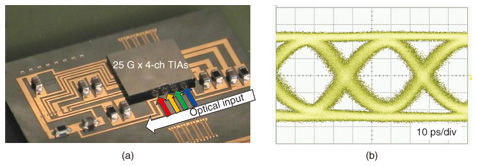
4. Integration of electronics on photonic chipAs mentioned in the previous section, it is very important to use TIAs to improve the receiver sensitivity. Generally, electrical wiring between a TIA and PD should be as short as possible, typically a few hundred micrometers or less for 25-Gbit/s signals. Conventionally, wire bonding technology is used to connect a TIA to a PD. In the wire bonding connection, however, it is difficult to shorten the wiring, and the frequency response is therefore easily degraded by parasitic impedances. The wiring should also be shortened for other high-speed electronics for photonic interfaces, for example, modulator drivers. In other words, the electronic components should be located as close as possible to the photonic ones. From this point of view, the electronics should be located on photonic chips. For this photonics-electronics convergence, electronics back-end processes should be performed on photonic chips, upon which the electronic wiring should be constructed and electronic chips mounted. The Si-based photonic platform is suitable for this kind of photonics-electronics convergence because it is very robust for electronics back-end processes. An example of photonics-electronics convergence for a WDM receiver system is shown in Fig. 12(a). Four-channel Si-based ring resonator wavelength filters and Ge PDs are monolithically integrated on a photonic chip. This photonic chip contains electronic wiring that includes transmission lines, capacitors, and resistors, as well as a four-channel TIA mounted using flip-chip bonding technology. The frequency response of the wiring between the TIA and PD is flat throughout a 40-GHz range. Thus, we obtained a very clear eye pattern of the TIA output for 25-Gbit/s signals, as shown in Fig. 12(b).
5. SummaryWe reported a Si-Ge-silica monolithic photonic integration platform for telecommunications applications. This platform enables monolithic integration of Si/Ge-based compact modulators/detectors and silica-based high-performance wavelength filters. The monolithic integration process features low-temperature silica film deposition by ECR PECVD so as not to damage the Si/Ge active devices. Since the right materials are applied for the right functions, the Si-Ge-silica platform can provide well-balanced performance for telecommunications applications, whose specifications are too strict for the conventional silicon-based photonic platform. We have developed various integrated photonic devices for broadband WDM applications using this platform. An integrated AWG-PD device works very well as a multichannel WDM receiver with a 400-Gbit/s transmission capacity. High-speed electronics can also be integrated on this Si-Ge-silica photonic platform. Thus, with the Si-Ge-silica monolithic photonic integration platform, we can construct a highly functional WDM photonic module with an electronic interface on one chip, which can be applied in compact, energy-efficient, and cost-effective photonic network systems. References
|
|||||||||||||||||||||||||||||||||||||