|
|||||||||||||||||||||||||||
|
|
|||||||||||||||||||||||||||
       |
Feature Articles: Frontiers of Quantum Optics Research at NTT Basic Research Laboratories Vol. 12, No. 9, pp. 8–13, Sept. 2014. https://doi.org/10.53829/ntr201409fa2 Photonic Quantum Information Devices Using Coupled-resonator Optical WaveguidesAbstractIntegrating a quantum circuit on a small photonic chip offers the promise of large-scale quantum information processing using photons. In this article, we review our research and development of integrated quantum information devices using silicon photonic crystal technology. Keywords: quantum information, photonic crystals, slow light
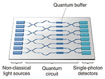
1. IntroductionPhotons are excellent carriers of qubits, which are substantial resources for quantum information processing (QIP) technologies [1]. The application of QIP includes quantum computation, where there are known tasks that can be performed significantly faster compared to what can be achieved on today’s conventional classical machines. The tasks could include simulation, factoring, searching, and so on. As is predicted from the current classical computers, it will be necessary to miniaturize and integrate QIP devices on a small chip. This implementation can be done by using integrated photonics technology such as silica-based planar lightwave circuits and silicon photonic circuits, which for many years have been developed for telecommunications applications by many institutions including NTT. For instance, we can achieve a quantum logic gate for quantum computation by exploiting directional couplers (beam splitters) [2], which are fundamental devices widely used in optical communication. Consequently, much research is being done on developing a QIP system using integrated photonics technologies. A typical integrated quantum system is schematically depicted in Fig. 1. The system has three main building blocks: quantum light sources that generate non-classical light such as a single photon or entangled photons [3, 4]; a linear-optical quantum circuit that manipulates quantum states encoded in the photon’s physical degrees of freedom [5]; and single-photon detectors. Here, we achieved a light source and a new component for the circuit using silicon photonic crystal nanocavities [6]. Thanks to a strong light confinement feature achieved in photonic crystals, we realized ultra-compact photonic components on a chip. Moreover, we successfully improved the efficiency and the functionality of those devices by exploiting the slow-light mode that arises in nanoscale photonic crystals [7, 8].
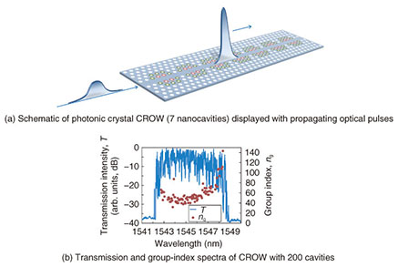
2. Silicon photonic crystal coupled-resonator optical waveguidesWe use coupled-resonator optical waveguides (CROWs) consisting of photonic crystal nanocavities [5]. A CROW is a waveguide consisting of optical cavities that are nearest-neighbour coupled along a one-dimensional direction. The chain of optical cavities induces a collectively resonant mode, whose properties (bandwidth and dispersion) can be strongly modulated by controlling the strength of the inter-cavity couplings. This feature is unlike that of conventional optical waveguides whose guiding properties are dominated by lateral confinement structures. Because of this feature, we can design CROWs to realize a large-bandwidth waveguide for high-speed signal transmission, or a small-group velocity waveguide for buffering optical signals depending on the application. A schematic of our photonic crystal CROW is shown in Fig. 2(a). The CROW is fabricated on a 210-nm-thick silicon top layer of a silicon-on-insulator wafer. The photonic crystal is formed by triangular-lattice air holes 105 nm in diameter and with a lattice constant a of 420 nm. Each optical cavity is formed by the local width modulation of a line defect in the photonic crystal. The colored holes are shifted by a few nanometers in-plane toward outside. This width modulation yields a cavity mode with a cavity Q greater than one million [9]. We show transmission and group index spectra of our CROW in Fig. 2(b). Here, the group index ng is the group velocity in a vacuum c divided by the group velocity in the media. The CROW exhibits ng ≈ 40 in a passband as wide as 6 nm. The CROW has low loss thanks to the ultrahigh Q of individual cavities, which suppresses the out-of-plane scattering of the propagating optical field [9]. In addition, our nanofabrication accuracy is high enough that the propagation mode is less influenced by a localized mode caused by structural disorder [10]. As a result, we successfully achieved light propagation in a CROW up to 400 cavities, which is the largest scale to date.
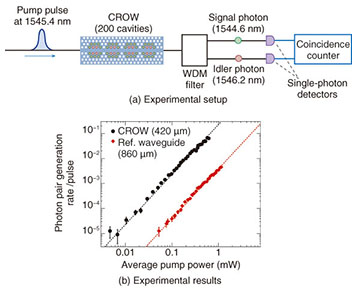
3. Slow-light-enhanced generation of correlated photon pairsThe non-classical light source includes a correlated photon pair source, which generates a pair of photons that correlate in their generation time. For the generation, we can use a spontaneous four-wave mixing (SFWM) process, which is a third-order nonlinear effect. By injecting a pump laser with an appropriate wavelength into a nonlinear waveguide, we can create correlated twin photons after annihilating two photons in the pump field. This process obeys the conservation law of energy and momentum between the four involved photons. Here, we call the generated twin photons a signal photon and an idler photon. We can enhance the nonlinear optical effect per unit device size using slow-light propagation. This is because, first, the slow-light mode simply prolongs the light-matter interaction time by a factor of ng. Second, the slow-light mode compresses the optical field along the propagation axis such that its peak intensity increases by a factor of ng. As a result, the nonlinear constant γ (/W/m), which is a typical measure of the strength of waveguide nonlinearity, is proportional to ng2. Our experiment demonstrated γ = 13,000/W/m at ng ≈ 49 [11]. This value is the highest ever reported in any silicon-core nonlinear waveguides. This value also indicates that a 1-mm-long CROW yields nonlinearity that is as strong as that of a 10-km-long optical fiber. We attempted to improve the generation efficiency of photon pairs via SFWM using the slow-light effect. The experimental setup is schematically depicted in Fig. 3(a). We injected pump pulses with a center wavelength of 1545.4 nm to the CROW. Photon pairs generated in the CROW are separated by the wavelength-division-multiplexing (WDM) filter into two different optical paths, and subsequently received by the single-photon counting modules (SPCMs). The pair generation rate can be estimated by a coincidence measurement of the detection signals from the two SPCMs. The experimental results are shown in Fig. 3(b). We see that the generation rate is proportional to the square of the pump power. This is because the photon pair generation in SFWM is caused by the simultaneous annihilation of two photons in the pump field. We also performed the same experiment using a reference line-defect photonic crystal waveguide (ng ≈ 6) fabricated on the same chip. From Fig. 3(b), we observe that the pair generation rate from the CROW is two orders of magnitude larger than that from the reference waveguide. The enhancement can be explained by the differences in the ng values and the length of the waveguides. We obtained a pair generation rate of 0.1 per pump pulse at an average pump power of less than 1 mW; this generation rate is high enough for the photon pair source based on spontaneous processes. Thus, we successfully enhanced the photon pair generation rate by almost 100 times using the slow-light effect in the CROW [6].
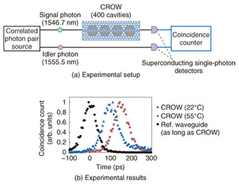
We further demonstrated the efficient generation of entangled photons from the CROW [12]. Quantum entanglement is a key resource for many QIP protocols. This is a key technology to realize a compact on-chip entangled photon source required for large-scale quantum information systems. 4. On-chip quantum bufferThe quantum circuit shown in Fig. 1 consists of arithmetic elements such as quantum logic gates, for which we can use the quantum interference effect between two identical photons on a directional coupler (i.e., beam splitter) [2]. In doing so, we have to synchronize the arrival times of the photons generated from different sources at the directional coupler. Such synchronization can be achieved by means of a quantum buffer, which is capable of actively controlling the propagation time of a photon without degrading its quantum properties. We created a quantum buffer using the photonic crystal CROW [8]. The experimental setup is shown in Fig. 4(a). We inserted a CROW in the optical path of the signal photon before the photon pair detection at the SPCMs. We performed the coincidence measurement and obtain an arrival time difference of the correlated photons. We observed this arrival time difference with and without the CROW. To obtain the high temporal resolution necessary to discriminate the arrival time difference, we used superconducting single-photon detectors, which have a high temporal resolution as well as a high signal-to-noise ratio. The experimental result is shown in Fig. 4(b). The horizontal axis indicates the arrival time difference of the pair of photons; that is, it indicates the extent of the delay of the signal photons with respect to the arrival of the idler photons. The vertical axis is a coincidence count normalized with respect to the peak count rate. For a reference, we used the same line-defect photonic crystal waveguide as the one used in the experiment described in section 3. We set the arrival time difference for the reference waveguide to the origin of the horizontal axis. By replacing the reference waveguide with the CROW, we observed a clear delay—as much as 150 ps—of the arrival time of the signal photons. Hence, we successfully demonstrated a single-photon delay line on a chip. A clear transmission signal was obtained even with the CROW with 400 cavities thanks to the ultrahigh Q value of each photonic crystal cavity.
We conducted another experiment to actively control the buffering time. To achieve this, we exploited the wavelength dependence of ng shown in Fig. 2(b). The ng spectrum can be shifted along the wavelength axis simply by varying the temperature of the CROW. In this way, we can change the ng of the CROW without changing the wavelength of the signal photon. We show the coincidence waveform at the chip temperature of 55°C. The delay time is approximately 103 ps. Thus, we achieved delay tuning of the single-photon wave packets over approximately 50 ps. Furthermore, we also confirmed that the chip was able to buffer one of the entangled photons. The time-bin entanglement encoded in the correlated photons was successfully stored for 150 ps without any degradation of the degree of entanglement. This experiment suggests that we can readily utilize our on-chip quantum buffer for storing and retrieving photons that possess qubit information. 5. Summary and outlookWe reported on-chip quantum photonic devices using the slow-light effect in a silicon photonic crystal CROW. We have shown that photonic crystal technology can increase the efficiency and functionality of building blocks for integrated photonic quantum information processing. To fully achieve the integrated QIP system, it is also necessary to integrate a WDM filter for the photon pair source and single-photon detectors. We aim to monolithically integrate the quantum subsystems in our efforts to realize a large-scale photonic QIP system. AcknowledgementThis work was partly supported by Grants-in-Aid for Scientific Research (Kakenhi) from the Japan Society for the Promotion of Science (22360034). References
|
||||||||||||||||||||||||||