|
|||||||||||||
|
|
|||||||||||||
       |
Feature Articles: Frontiers of Quantum Optics Research at NTT Basic Research Laboratories Vol. 12, No. 9, pp. 29–33, Sept. 2014. https://doi.org/10.53829/ntr201409fa6 A Bose-Einstein Condensate Achieved on a Persistent-supercurrent Atom ChipAbstractA persistent-supercurrent atom chip is a quantum device designed with a view to transcending the limits of conventional technologies by employing some of the significant properties of quantum mechanics. We have applied this novel technique to achieve an atomic gas in a macroscopic quantum state in the vicinity of a solid-state surface. In this article, we review a technique for making an extremely stable Bose-Einstein condensate above a chip surface and describe our attempts to overcome several unpredicted problems introduced by superconductivity. Keywords: atom chip, superconductor, quantum devices
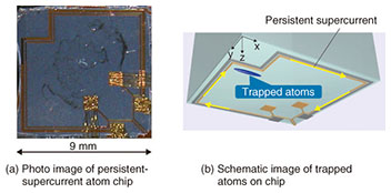
1. IntroductionQuantum mechanics, the branch of physics dealing with the small-scale world of atoms and photons, provides peculiar outcomes that are counterintuitive to those familiar with the macroscopic world. A probabilistic state is a good example; in addition to definite states of 0 or 1, quantum mechanics allows the existence of probabilistic states with superpositions of 0 and 1. Such non-intuitive quantum properties are strongly expected to be a key resource for realizing ultra-high-speed calculations and ultimately secure quantum cryptography. The realization of these transcendent technologies requires the development of quantum devices, e.g., quantum memories and gates, with which we can store and operate quantum states. Quantum device research on photons, ions, semiconductors, and superconductors is underway throughout the world out of both purely scientific interest and the desire to surpass classical technologies. We are focusing our research on ultra-cold atoms with which we can potentially realize scalable quantum devices. In 2007 we detailed our prospects for developing atomic quantum devices by introducing a persistent-supercurrent atom chip [1]. In that article, we mentioned techniques for decelerating the velocity of atoms from about 300 m/s to 0 m/s with lasers, and for holding the atoms in a stable magnetic potential generated by a persistent supercurrent. In this article, we describe the further progress that we have made with the persistent-supercurrent atom chip. We have succeeded in achieving atomic gas in a macroscopic quantum state, i.e., a Bose-Einstein condensate (BEC), by taking advantage of the stable potential near the surface of a chip. Achieving a BEC was not straightforward; we encountered a lot of strange superconductor behavior and struggled, ultimately successfully, to find the correct route. An atomic BEC is an isolated pure state with many controllable parameters, and it is attracting considerable interest in the field of science. Our recent achievement of a stable BEC on a chip is regarded as a technical breakthrough that is paving the way for BEC applications in engineering. The initialization of quantum devices is a promising target of such applications. An atomic BEC is analogous to lasers in electromagnetic waves; it exhibits good coherence in de Broglie waves, and a single coherent state constituted with a large number of atoms is useful for quantum memory and gate operations. Although our research still requires further improvement, we summarize our progress here and explain the novel techniques we have achieved so far along with the efforts we have made to overcome unpredictable problems encountered during the development. 2. Peculiar behavior of superconducting atom chipsWhen we succeeded in trapping atoms with our persistent-supercurrent atom chips (Fig. 1) [2], we believed that the trap had to be extremely stable even in the vicinity of a solid-state surface because spin-flip loss is suppressed. To evaluate the performance of our superconducting atom chip, we examined its trapping stability and found that the trap lifetime was ten times that achieved with conventional techniques [3]. This result was clearly an improvement; however, it did not satisfy us because the lifetime was much shorter than we had expected. According to our theoretical calculations, the trapping lifetime of superconducting atom chips should be more than 10,000 times longer than that of normal conducting atom chips. In addition to the unexpectedly short lifetime, we also encountered unreasonable fluctuations in the lifetime measurements. These strange results were caused by an interesting property of superconducting materials, which we came to understand later, as described below.
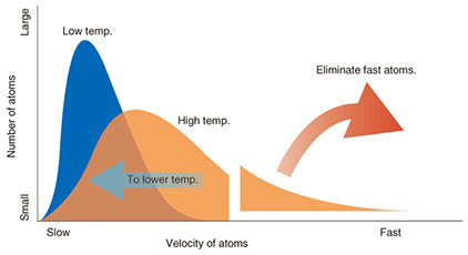
Type II superconductors, with which we can drive a relatively large current and achieve strong confinement in a magnetic potential, are advantageous for use in atom chip experiments. As is well known, magnetic fluxes penetrate and remain in the body of type II superconductors. The flux penetration condition strongly depends on the intensity of the magnetic field applied from outside the superconductor, but the critical field value is about ten times larger than the value that we usually use in cold atom experiments. For this reason we disregarded the influence of magnetic-flux penetration into our type II superconducting circuit on a chip. As we found out later, the flux penetration criterion also depends on the thickness of the superconductor. With a thin film superconductor, the critical field for the flux penetration becomes much smaller than that of a bulk superconductor. Moreover, the penetrated magnetic fluxes change their patterns from homogeneous to dendritic configurations depending on the temperature and the magnetic field around the superconducting film. We encountered these peculiar and interesting phenomena when measuring atomic clouds with our superconducting atom chips [4]. At first we thought we might have found an unknown physical property. However, the phenomenon, which is called dendritic flux avalanche, had been observed only a few years before with a completely different technique. Once the mechanism of the problem was clarified, it was not that difficult to come up with tactics to overcome the problem. Controlling the chip temperature was the key to achieving stable operation of superconducting atom chips. To give the superconductor zero resistivity, we have to cool the chip below a critical temperature Tc. To keep the penetrated magnetic fluxes stable, the chip temperature should be higher than another critical temperature Td, at which the penetrated magnetic fluxes change to a dendritic pattern. By controlling the chip temperature so that it was between Td and Tc, we succeeded in achieving an extremely stable magnetic potential with our superconducting atom chip. 3. Evaporative cooling with a superconducting closed loop circuitThe first step in making a BEC is to create a stable atomic cloud; the next step is to further reduce the atomic cloud temperature through evaporative cooling. The mechanism of evaporative cooling is easily understood with the help of the intuitive image shown in Fig. 2. First, energetic atoms are removed from the atomic cloud, and the remaining atoms then start to thermalize into an equilibrium state at a lower temperature through the atom interaction. In this process, a radio-frequency (RF) magnetic field is used in order to eliminate high-energy atoms from the atomic cloud through the use of resonant action. In atom chip experiments, the RF magnetic field is usually generated by an alternating current (AC) on a chip circuit. For the first trial in our experiment, we employed the same technique and introduced an AC into our chip circuit to generate an RF magnetic field. The result was poor; both the high-energy atoms and all the other atoms escaped from the trapping potential in a short period. As is usual when developing a new technology, unpredicted problems can be introduced by employing an old method; the combination of our novel superconducting circuit and a conventional AC on a chip circuit resulted in a problem arising from the unwanted behavior of the trapping potential.
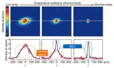
With a superconducting closed loop circuit, the total magnetic flux or fluxoid (the sum of the magnetic field applied from outside and the field generated by the circuit current) inside the closed loop circuit is preserved, which is called fluxoid conservation. By properly applying this natural law, we can drive a persistent current into a closed loop circuit without connecting a power supply to the chip circuit. This is a key advantage of our technique because it suppresses the electromagnetic noise arriving from the environment through conducting wires. However, the natural principle also means that a current in a closed loop circuit is sensitive to a magnetic field penetrating through the circuit itself. In our experiment, an RF magnetic field generated by an AC on a chip penetrated the closed loop circuit and modified the persistent current. The modulated persistent current vibrated the trapping potential and resulted in atoms being lost from the potential. Finally, we came to understand that the RF magnetic field for evaporation should be applied parallel to the chip surface to avoid field penetration of the closed-loop circuit. To realize this configuration, we attached an independent single-loop RF coil perpendicularly to the chip circuit, and succeeded in evaporatively cooling the atomic cloud to form a BEC by removing only the energetic atoms from the trapping potential [5]. 4. BEC measurementsWe investigated the BEC on a persistent-supercurrent atom chip with a time-of-flight imaging technique. First, an atomic cloud was released from the trapping potential, and then an absorption image was captured as a shadow of the atomic cloud, which was expanding depending on the initial temperature in the trap. Typical images obtained before and after the BEC transition are shown in Fig. 3. The left image shows a relatively large distribution of the atomic cloud, which suggests a high temperature, whereas the right image shows a small distribution, suggesting a low temperature. In the center image, the created BEC is observed as a higher density at the center of the atomic cloud. The image on the right shows that almost all of the 100,000 atoms are condensed into the potential ground state. The change in the atomic-cloud shape from a large horizontal configuration (left) to a small longitudinal one (right) is also apparent in this figure. This configuration change also proves that we were successful in achieving a BEC.
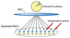
5. Future prospectsWe have achieved a BEC in the extremely stable potential of a persistent-supercurrent atom chip. The long coherence time for preserving fragile quantum states is outstanding compared with conventional technology. If we assume single atoms as single qubits, a BEC composed of 100,000 atoms is equivalent to a single package of 100,000 initialized qubits. The next step is to develop a technique for separating a BEC into several atomic clouds or single atoms and for controlling each atomic cloud independently. If we succeed in developing a technique such as that shown in Fig. 4, we will come very close to realizing atomic quantum devices.
References
|
||||||||||||