|
|||||||||||||||||||||||||
|
|
|||||||||||||||||||||||||
       |
Feature Articles: Frontier Research on Low-dimensional Semiconductor Physics Vol. 13, No. 8, pp. 27–34, Aug. 2015. https://doi.org/10.53829/ntr201508fa6 Semiconductor Quantum Structures with Single-atom PrecisionAbstractAtom manipulation is a technology to assemble microstructures atom-by-atom by controlling the number of component atoms and their configuration. Combining this technology with the epitaxial growth of high quality semiconductor crystals makes it possible to uniformly manufacture and integrate quantum structures with single-atom precision. This technological innovation is expected to enable the next generation of electronics to overcome the limits of conventional silicon technology. In this article, atom manipulation of quantum structures at a compound semiconductor surface is reviewed, and a typical example is described—the fabrication of an ultimately precise quantum dot and quantum dot molecules. Keywords: atom manipulation, STM, quantum structure
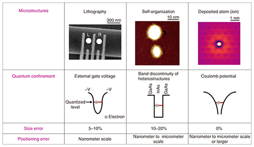
1. IntroductionWe have access to enormous amounts of information on the Internet these days. We can casually observe street views of arbitrary places almost anywhere on Earth. In the bygone era of telephone cards and message dial services, such a ubiquitous and interactive service was only a dream. Microfabrication is one of the technologies that has played a leading role in making this dream come true in our daily lives. Semiconductor microfabrication technology has steadily progressed following Moore’s law, which predicts that the number of transistors in an integrated circuit (IC) will double approximately every two years. However, this performance improvement of ICs is expected to come to an end in the near future because of quantum mechanical leakage current manifested by the miniaturization. Extensive research has been ongoing to find a way to overcome this limitation, and some studies have explored novel electric circuits that exploit evident quantum mechanical phenomena. To achieve such quantum mechanical electric circuits, microstructures called quantum structures are used in order to take advantage of the quantum mechanical behavior of electrons. A nanostructure*1, one such microstructure, is considered to be a fundamental structure in which quantum behavior becomes the driving mechanism of novel electric circuits. The kinetics of a quantum shows a wave-particle duality, a concept that consists of the properties of a particle (kinetic momentum p = mv, where m and v are the mass and the velocity of the quantum) characterized by Newton’s equation of motion, and the properties of a wave (wavelength λ) characterized by the Schrödinger equation. This λ is called the de Broglie wavelength*2 and is estimated as λ = h / mv (h: Planck constant). The de Broglie wavelength of an electron in a semiconductor is roughly a few tens of nanometers (1 nm = 10−9 m). In contrast, the distance between the nearest-neighbor atoms in solids is of the order of 0.25 nm, which corresponds to about 1% of λ. The impact of a microfabrication error becomes more critical as the manufactured device becomes smaller. This means that the electronic states in quantum structures are highly sensitive to a structural fabrication error on the order of a few atoms. The present error status of microfabricated nanostructures is shown in Fig. 1. It is clear that conventional microfabrication methods such as lithography and self-organization result in unavoidable variations comparable to or larger than the required precision in size and positioning. The effects of the inevitable processing errors make the device characteristics considerably inaccurate and problematic. Thus, to precisely control quantum mechanical electrons, microfabrication technology for quantum structures needs to have a degree of accuracy with the precision of a natural atom, which is the fundamental unit of matter.
In natural atoms, the Coulomb potential caused by the nucleus determines the quantum states of confined electrons. Since the potential form is determined by the atomic number, the electronic states are identical in each atom. Therefore, in the deposition process of atoms targeting a specific position on a solid crystal surface, the size error of the confinement structure by atoms becomes zero (Fig. 1), except for the positioning errors induced by focusing accuracy and thermodynamic uncertainty [1]. Atom manipulation is a method of flexible positioning of atoms on a surface. The practicability was demonstrated [2] soon after the invention of the scanning tunneling microscope (STM) [3]. If the positioning uncertainty of the focused atom beam process can be corrected by atom manipulation after the deposition process, we can solve the positioning error problem by utilizing the size-error-free feature of natural atoms. In other words, atom manipulation is a key microfabrication technique with ultimate precision.
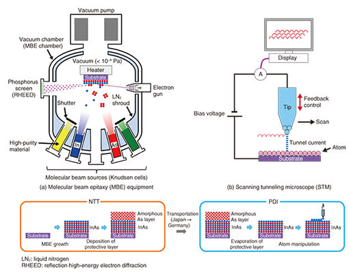
2. Experimental methodAs a template for the atom manipulation, we used a (111)A-oriented surface of indium arsenide (InAs) crystal. InAs is a compound semiconductor composed of indium (In) and arsenic (As). It is one of the most important materials in high-speed electronic and infrared photonic devices. A high-quality InAs single-crystal thin film was grown on the (111)A-oriented substrate with atomically controlled thickness by using the crystal growth technique molecular beam epitaxy (MBE), as shown in Fig. 2(a). Epitaxy refers to single-crystal growth with one particular crystallographic orientation on a substrate. MBE is a vapor growth method, which performs the epitaxy by exposing the substrate to beams of atomic or molecular gases of high purity materials to the substrate under an ultra-high vacuum of 10−8 Pa or less. The MBE method can grow semiconductor crystals with very high purity and crystallinity. After the growth, the grown InAs surface was covered by a protective film (amorphous As). Then the sample was sent from NTT to the Paul-Drude-Institut für Festkörperelektronik (PDI) in Germany. At PDI, the protective film was removed in an ultra-high vacuum to recover the clean (111)A surface, and the sample was loaded into an STM operated at a sample temperature of 5 K. An STM is an electron microscope in which an atomically sharpened conductive needle (tip) is scanned above the conductive sample surface. The tip probes a tunneling current by applying a voltage difference between the tip and the sample surface at a distance of 1 nm or less, as shown in Fig. 2(b). Through signal processing of the measured tunneling current, the STM visualizes the local electronic states to observe the surface atoms.
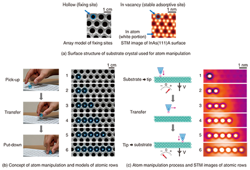
NTT and PDI have collaboratively developed atom manipulation at semiconductor surfaces using a low-temperature STM as a new approach to surpass conventional nanostructure fabrication technologies. Our achievements demonstrate that an international collaborative research project that combines individual skills and experience is effective for advancing science and technology. 3. Atom manipulation on semiconductor surfacesSurface atoms are arranged periodically on a semiconductor surface. Therefore, stable adsorptive sites of adsorbates also form periodic arrays. By using this periodicity, we can use the crystal substrate as a template to precisely control the structure formation by placing individual atoms at specific well-defined adsorptive sites. After the protective layer is removed, the (111)A surface recovers intrinsic hollow sites caused by periodic vacancies of surface In atoms at a distance of 0.857 nm. This surface structure is equivalent to that at the MBE-grown surface, as shown in Fig. 3(a). These hollow sites work as stable adsorptive sites. The concept of atom manipulation and some models of atomic chains are shown in Fig. 3(b). In the atom manipulation process, the STM tip is used to pick up target atoms from the surface one by one and put them down in the designated position as the building blocks to form well-tailored nanostructures of atoms. The manipulated In adatoms are those that remain at the surface after the MBE growth [4]. The pick-up process and the put-down process are controlled by the applied sample bias voltage V. At the experimental substrate temperature of 5 K, thermal diffusion of adatoms at the sample surface is suppressed, and individual manipulated atoms are fixed stably at the positioned sites. We manufactured atomic chains (1 ≤ N (the number of atoms) ≤ 6) by arranging each In atom one-by-one in a line at the (111)A surface, as shown in Fig. 3(c) [5]. Precise and reproducible atomic configurations were possible because of the periodic and symmetric arrangement of stable adsorptive sites.
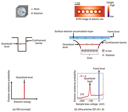
In addition to enabling microfabrication of quantum devices with single-atom precision, atom manipulation is advantageous in producing novel assemblies of integrated atoms, which do not exist in nature and are also not possible by means of chemical reaction. This is a very attractive subject that warrants further study. We expect that atom manipulation on semiconductor substrates will provide a novel aspect to our understanding of the physical and chemical properties of materials. 4. Quantum structures with ultimate precision4.1 Ultra-precise quantum dotsThe current atom manipulation technology enables us to flexibly implement quantum dots (QDs) with properties identical to those of natural atoms at the semiconductor substrate surface with single-atom precision of position and configuration. At the InAs surface, the indium (In) adatom is self-ionized to become a +1 charged ion that releases an electron to the substrate. Thus, a row of such ions behaves as a core, which confines electronic states at the semiconductor surface to the induced local Coulomb potential. This potential is well-defined, like that of a natural atom. These adatom-assembled structures work as ultra-precise QDs with excellent uniform properties. A QD is a microscopic structure that confines electrons in a narrow, nanometer-scale space with length, width, and height all comparable to or smaller than the de Broglie wavelength of free electrons (1–100 nm), making quantum mechanical effects evident. The concept of the QD is shown in Fig. 4(a). The QD is an essential component of electronic and optical semiconductor devices and has been extensively studied in the information technology field as a key element for developing a quantum computer. The electrons confined to a QD obey quantum mechanical statistics and form discrete energy levels similar to those of natural atoms. Moreover, QDs reproduce intrinsic properties of natural atoms such as the electron shell structure and Hund’s rules [6]. Thus, a semiconductor QD is often called an artificial atom (which is not to be confused with an artificial element). The experimental results for a QD with N = 6 are shown in Fig. 4(b). Electrons are attracted to the core of ionized adatom rows. The spectral peak indicates that the free electronic states at the semiconductor substrate are confined, and a quantized level is obtained below the Fermi level*3. The discrete peak spectra of QDs (6 ≤ N ≤ 25) were characterized experimentally [7].
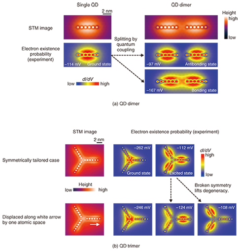
4.2 Integration of ultra-precise quantum dotsAn artificial molecule, a microscopic structure made of artificial atoms, shows properties similar to those of a natural molecule. When two ultra-precise QDs (N = 6) are coupled as shown in Fig. 5(a), molecular electronic states appear as a result of the interaction between individual quantized states in the QDs [6]. The observed states correspond to a bonding state and an antibonding state, similar to a natural dimer molecule. Here, the electron existence probability maps (spatial distributions of the local density of states) were visualized by measuring the differential conductance (dI / dV) signal of the tunneling current I at a given sample bias voltage V. When exactly the same artificial molecule structures were fabricated, the standard deviation of the splitting energy between the bonding and antibonding levels was about 1 meV. This means that the fluctuation of the quantization characteristics is equivalent to the unavoidable thermal fluctuation limit at the substrate temperature of 5 K (3.5kBT / 2 = 0.8 meV; kB: Boltzmann constant). This confirms that the reproducibility of quantization characteristics is excellent. It should be emphasized that it would not be possible to substantially demonstrate the characteristics of the ultra-precise quantum structures fabricated using the atom manipulation technique if there were any fluctuations due to defects or impurities. We were able to experimentally confirm the excellent fabrication accuracy by atom manipulation only because the quality of the MBE-grown semiconductor crystal was sufficiently high. This indicates that very minute semiconductor quantum structures require the synergistic effect of combining the extremely high processing accuracy at atomic-scale precision and the high crystallinity of the semiconductor crystal. The availability of such ultra-precise quantum structures enables us to manufacture ultimate quantum devices with atomic-level reproducibility like an array of quantum bits with uniform functions, which have not yet been achievable because of statistical errors in structural fluctuations. Furthermore, integration and control of these precise nanostructures will help us to develop a quantum computer and the next generation of technology to overcome the limits of conventional silicon technology. When three ultra-precise QDs (N = 6) are combined as shown in Fig. 5(b), they form a nanostructure corresponding to a QD trimer molecule [6]. When one of the component QDs was displaced at a distance of one adsorptive site (0.857 nm), and thereby the rotational symmetry was broken, tunneling spectroscopy measurements revealed that the doubly degenerated excited level split into two individual levels. This infers that the electronic structure of the symmetric QD trimer consists of molecular levels, as is expected from a triatomic molecule of threefold symmetry. It also shows that an atomic-level error of the quantum structure has a crucial effect on the quantum characteristics.
From the viewpoint of device integration, this QD trimer is regarded as a semiconductor structure made of three QDs integrated in a 10 × 10 nm square area. If the degree of integration is estimated by assuming that one QD corresponds to one transistor, the degree is about 1000 times as high as that of conventional ICs, though it is limited to a local area. This indicates that the QD trimer molecule in Fig. 5(b) can be considered a mock-up of an ultimately integrated semiconductor microstructure. The thermal de Broglie wavelength λD (defined by λD = h / The design and analysis of the artificial atoms and molecules were performed by doing theoretical first-principles calculations at the Naval Research Laboratory (NRL) in the USA in collaboration with PDI. This theoretical analysis enabled us to confirm that the confined states in QDs originate from the intrinsic electronic states of the semiconductor substrate, not from the atomic orbitals of In adatoms.
5. Future perspectivesAt present, STM-based atom manipulation is the sole technology for fabricating ultra-precise quantum structures with respect to position and configuration. We expect that the present achievements will open the door to developing new electronics technology by combining atomic and molecular electronics with semiconductor thin film technology. However, the throughput of atom manipulation, namely the efficiency of manufacturing nanostructures per unit time, is inferior to that of conventional lithography technologies [8]. When this drawback is overcome and the fabrication and characterization of quantum structures with atomic precision become possible at the semiconductor substrate surface, we will be a giant step closer toward realizing a new IC technology through the fusion of wafer-level semiconductor technology and atomic and molecular electronics. By exploring novel properties of many integrated atoms and their interaction with semiconductor heterostructures, we plan to develop architectures for quantum computers and high-performance semiconductor devices composed of well-defined semiconductor nanostructures with robust fidelity. Further study will bring many benefits to a broad range of science and technology fields. References
|
||||||||||||||||||||||||