|
|||
|
|
|||
|
Feature Articles: Frontier Research on Low-dimensional Semiconductor Physics Vol. 13, No. 8, pp. 35–41, Aug. 2015. https://doi.org/10.53829/ntr201508fa7 Creating a Topological Insulator Using Semiconductor HeterostructuresAbstractTopological insulators are new states of matter that cannot be classified into any existing categories of materials. They have attracted much attention for their potential use in electronic and quantum computing devices because of their specific electron transport properties. In this article, we describe how we created an artificial topological insulator using a heterostructure comprising common semiconductor materials. Keywords: semiconductor heterostructure, topological insulator, edge channel  1. IntroductionWe have recently seen a new movement in materials science to classify materials from the viewpoint of topology. In the process, new states of matter have been found, which cannot be classified into existing categories of materials. One such state is the topological insulator (TI), which has an insulating phase with a topology different from that of normal insulators. Mathematically, a state cannot continuously transit between different topologies and is therefore necessarily broken at the boundary (Fig. 1). In an analogous way, the insulating state in TIs cannot continue to the normal insulating state outside, and it is therefore necessary to break the insulating states. As a result, a conductive channel arises at the boundary of a TI. This topologically protected conductive channel is expected to have low power consumption or specific transport properties, and thus, TIs have attracted a great deal of attention as a new type of electronic material.
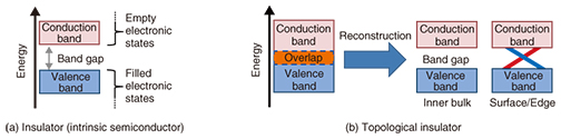
Several TIs have been confirmed experimentally, for example, Bi2Se3 and HgTe. However, these materials are not common in industry, and specific know-how is necessary to achieve their crystal growth. They have a distinct energy band structure by nature, which is what realizes a TI (discussed later). In contrast, we created an artificial TI by using a semiconductor heterostructure comprising indium arsenide (InAs) and gallium antimonide (GaSb) [1], which are commonly used industrially. Taking advantage of the highly developed semiconductor technology will make it possible to carry out detailed clarifications and to implement various device applications of TIs. 2. Topological insulatorWhen atoms are condensed and crystallized, the electron orbits for each atom are hybridized. As a result, electronic states called energy bands are formed due to the periodicities of the crystal. The energy band accumulates electrons from the lower energy side. When one energy band is completely filled by the electrons and the upper energy band is empty, the state of the matter becomes an insulator (Fig. 2). The filled energy band is called the valence band, and the upper empty energy band is called the conduction band. The gap between these energy bands is called the band gap. This is the situation in an intrinsic semiconductor. At low temperatures, thermal excitation of electrons from the valence band to the conduction band is suppressed. This state results in an insulator.
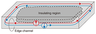
In TIs, the conduction and valence bands overlap energetically. The wave functions in each band are hybridized based on the relativistic interaction. As a result, the energy gap is reopened and the conduction and valence bands are reconstructed. When the reconstructed valence band is completely filled with electrons and the conduction band is empty, an insulator state exists. However, the topology of this state is different from that outside. Therefore, the band gap should be closed at the boundary. Electronic states connecting the valence and conduction bands appear as a conductive channel (red and blue lines in Fig. 2(b)). For a three-dimensional (3D) TI, this conductive channel corresponds to the two-dimensional (2D) surface state. For a 2D TI, this channel corresponds to the edge channel. Singular electronic transport is expected due to the restriction of electron scattering. We have been investigating 2D TIs whose edge channel is composed of counter-propagating electron currents with opposite spin directions, which are called helical spin currents (Fig. 3). The topologically robust protection of the edge channel prevents the back scattering of electrons between counter-propagating currents in the edge channel with spin flip. As a result, dissipationless electron transport, that is, quantized conductance, should be achieved. In practice, a value very close to the quantized conductance has been observed in an HgTe/HgCdTe heterostructure, which is a representative 2D TI. In addition, at the junction between the helical spin current and the superconductor, a curious quasiparticle state called the Majorana fermion, which is simultaneously a particle and its antiparticle, is expected to be found. The Majorana fermion is promising as a quantum bit for fault-tolerant quantum computing.
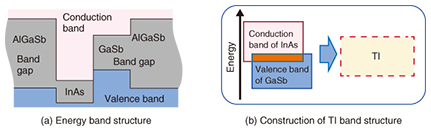
As described above, 2D TIs are promising for use in low-power-consumption devices, quantum computing, and spintronic devices. 3. InAs/GaSb heterostructureBoth InAs and GaSb are common and widely used semiconductors. When the heterojunction is made, the conduction band in InAs and the valence band in GaSb overlap energetically. After the layer thicknesses are optimized and the InAs/GaSb heterostructure is sandwiched between AlGaSb barrier layers, the energy band structure of TIs is artificially realized through the hybridization of the adjacent conduction and valence bands (Fig. 4). This heterostructure becomes a 2D TI because of the layer structure.
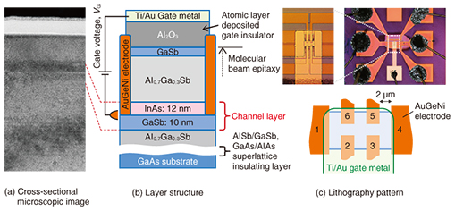
The structure of our sample is shown in Fig. 5. We grew the semiconductor layers using molecular beam epitaxy, which enables us to control each layer thickness to one atomic layer. We used photolithography and etching to fabricate a small device pattern, as shown in Fig. 5(c). Then, six electrodes were formed by evaporating AuGeNi alloy. An Al2O3 gate insulating layer was deposited by atomic layer deposition, and a Ti/Au top gate was evaporated. The electron density can be controlled by applying voltage between the gate and the InAs/GaSb channel layer. The TI is realized when the valence band is completely filled with electrons and the conduction band is empty.
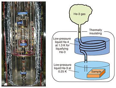
4. Low-temperature measurementSimilar to common insulators and intrinsic semiconductors, the insulating phase in a TI is broken by thermal electron excitation from the valence band to the conduction band. Therefore, to obtain the distinct transport properties of a TI, an extremely low temperature is necessary. Here, we used a He-3 (an isotope of helium) refrigerator (Fig. 6). In this refrigerator, He-3 gas is liquefied by low-pressure liquid He-4 (common helium), whose temperature is about 1.3 K. Then the pressure of the liquid He-3 is reduced. As a result, the lowest possible temperature of 0.25 K is obtained.
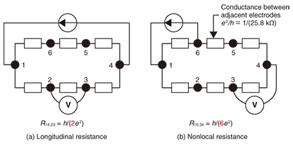
5. Confirmation of TIIn the 2D TI, the inner bulk part is insulating. The electron transport takes place through the edge channel between adjacent electrodes. Ideally, the conductance between the adjacent electrodes should be quantized conductance, e2/h, and the resistance should be its inverse, h/e2 ≈ 25.8 kΩ. The equivalent circuit models of the sample with six electrodes are shown in Fig. 7. Based on a simple resistance calculation, longitudinal resistance R14,23 = h/(2e2) ≈ 12.9 kΩ and, for example, nonlocal resistance R16,34 = h/(6e2) ≈ 4.3 kΩ are expected. In practice, however, electron scattering occurs for various reasons. Therefore, the conductance between the adjacent electrodes deviates from the quantized value.
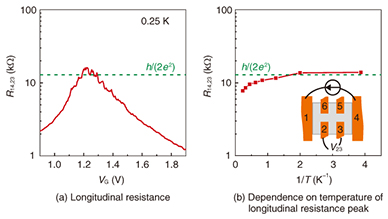
Longitudinal resistance (R14,23) experimentally obtained as a function of the gate voltage (VG) is shown in Fig. 8. The electron density is low on the low VG side, and there are unoccupied electron states (holes) in the valence band. The holes act as carriers with a positive charge and contribute to the electronic transport. Therefore, the inner bulk region is conductive, and R14,23 becomes low. In contrast, on the high VG side, electrons partially accumulate in the conduction band and act as conductive electrons, which also lowers R14,23. Around VG = 1.25 V, the valence band is completely filled with electrons and the conduction band is empty. There are no conductive electrons or holes in the inner bulk region. Therefore, R14,23 increases. The peak resistance of R14,23 is about 20 kΩ. If the sample were an intrinsic semiconductor, the resistance peak would become infinite. The finite resistance indicates that the sample has a conductive channel, and this resistance peak value is not far from that expected as quantized transport, h/(2e2). This suggests that the sample becomes a TI at this VG.
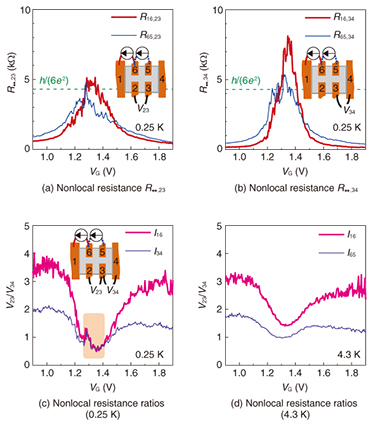
The dependence of the R14,23 peak on temperature is shown in Fig. 8(b), where the horizontal axis is the inverted temperature. On the high-temperature side (left side) the resistance peak is low. This is because the thermally excited electrons from the valence band to the conduction band and simultaneously generated holes in the valence band contribute to the electronic transport in the inner bulk region. The estimated energy gap from the slope in the high-temperature region is 0.18 meV (≈ 2.1 K). On the low-temperature side, the peak resistance approaches h/(2e2). In an attempt to obtain clear evidence for the TI, we measured nonlocal resistances. R16,23 and R65,23 as a function of VG are shown in Fig. 9(a). Here, Rij,kl (= Vkl/Iij) indicates that electrodes i and j are used for current (Iij) injection and ejection, and electrodes k and l are used for voltage (Vkl) measurement. Nonlocal resistances R16,34 and R65,34 are shown in Fig. 9(b). The resistance peaks deviate from the expected value h/(6e2) in the quantized transport. We could not confirm the realization of a TI from these results. Next, the nonlocal resistance ratios (voltage ratios between the adjacent electrode pairs, V23/V34) are plotted in Fig. 9(c). For the pink curve, the current is injected into electrode 1 and ejected from electrode 6. For the purple one, it is injected into 3 and ejected from 4. Around the resistance peak, these two curves completely agree with each other independently of the current injection/ejection path. We observed such agreement of the nonlocal resistance ratios between the adjacent voltage electrode pairs for all combinations of electrode arrangements. This indicates that the transport occurs only between adjacent electrodes; that is, the inner bulk region is insulating, and the transport is governed by the edge channel. Here, we can confirm the realization of a TI in the InAs/GaSb heterostructure. When the temperature is increased to 4.3 K, the agreement of the nonlocal resistance ratios disappears, as shown in Fig. 9(d). This indicates that the thermally excited carriers contribute to the transport in the inner bulk region.
6. Future prospectsBoth InAs and GaSb can achieve good electronic connections with ferromagnetics or superconductors. This is expected to lead to their application for spintronic or quantum information devices. In addition, our artificial TIs created using heterostructures between non-topological materials create the possibility of combining various materials, including insulators or metals, to achieve new TIs. Reference
|
|||