|
|||||||||||||||||||||||||
|
|
|||||||||||||||||||||||||
       |
Regular Articles Vol. 13, No. 10, pp. 43–49, Oct. 2015. https://doi.org/10.53829/ntr201510ra1 High-sensitivity Avalanche Photodiode and Receiver Optical Subassembly Technology for
|
||||||||||||||||||||||||
 |
 |
1. Introduction
The rapid increase in the capacity of communication networks has led to many new services. To handle the growing amount of transmitted data, the Ethernet standard has been repeatedly extended [1], and faster and faster interface speeds are necessary in order to cope with this trend. In particular, datacenters will need to deal with ever-increasing amounts of data in limited areas, and at the same time, the capacity of optical components and reductions in their size and power consumption will be urgently required. In addition, the transmission distance of 100-Gbit/s Ethernet systems will also need to be extended in order to meet the requirements for future application areas. Extending the reach beyond 10 km is very important for telecom carriers because it will enable most inter-building networks to be covered.
The key to extending the distance is the optical receiver because the launch power of the laser diode in the transmitter is limited. A schematic image of a 100-Gbit/s Ethernet 10-km transmission system (100GBASE-LR4) that uses a transmission optical subassembly (TOSA) and receiver optical subassembly (ROSA) is shown in Fig. 1(a). A typical ROSA includes a PIN photodiode to convert optical signals to electrical signals. The receiver sensitivity of a ROSA is limited in the system, and therefore, to extend the transmission distance, it is necessary to use an optical amplifier such as a semiconductor optical amplifier (SOA) in front of the ROSA, as shown in Fig. 1(b). However, in this configuration, the receiver module size cannot be reduced enough to keep up with the expected size of packages such as that of a CFP4 transceiver. In addition, an SOA consumes as much as several watts of power and enlarges the footprint.
Thus, to provide a means of improving the sensitivity without increasing the package size, we proposed a novel high-speed avalanche photodiode (APD) [2], as shown in Fig. 1(c). An APD has an internal gain that improves the sensitivity by several decibels compared to that of a PIN photodiode. Our APD, called an inverted p-down APD, has achieved a high multiplied responsivity-bandwidth product of 18.5 × 9.1 = 168 A/W·GHz [3] and can operate with a bandwidth large enough for receiving 25-Gbit/s data. In this article, we describe the design and fabrication of the high-speed, stable APD and the results of applying it to a 100-Gbit/s four-channel APD-ROSA.
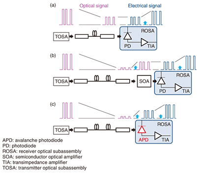
Fig. 1. 100-Gbit/s Ethernet transmission systems using TOSA and ROSA.
2. Inverted p-down APD
In addition to large bandwidth and high responsivity, the reliability and stability of an APD are the most important factors for its practical application, since a high applied voltage is necessary to obtain sufficient internal gain. We have devised a simple new APD structure, the inverted p-down APD, that is suitable for even higher speeds by scaling the structure down. The simple structure confines the electric field, which makes it possible to obtain good stability.
A schematic cross section of our APD is shown in Fig. 2(a). The epitaxial layers were grown on a semi-insulating InP substrate by using MOCVD (metal organic chemical vapor deposition). The APD structure consists of a p-doped contact layer, p-doped and undoped InGaAs absorption layers, an InAlAs avalanche layer sandwiched between p- and n-doped field control layers, and an n-doped contact layer.
Although there is a trade-off between bandwidth and responsivity in an APD, we optimize the thickness relationship between the p-doped and undoped absorption layers to relax the trade-off, in accordance with the concept of MIC (maximized induced current) design [4]. This is necessary because the two types of photo-excited carriers, namely holes and electrons, are transported through the p-doped and undoped layers by different mechanisms. We show how the calculated responsivity and the calculated intrinsic 3-dB-down bandwidth for a multiplication factor (M) of 1 varies with the total thickness of the absorption layer in Figs. 2(b) and 2(c). The optimum intrinsic 3-dB-down bandwidth was achieved by tuning the proportion of the total absorption layer occupied by p-doped absorption. For a speed of 25 Gbit/s, a total thickness of 1.0 µm provides a sufficiently large bandwidth and a high responsivity of 0.9 A/W.
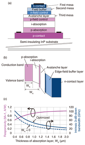
Fig. 2. (a) Schematic cross section of inverted p-down APD with triple mesa. (b) Parameters for calculation and (c) calculated responsivity (M = 1) and 3-dB-down bandwidth (M = 1), considered only in terms of intrinsic carrier transit time in absorption layer against total thickness of absorption layer.
Furthermore, the gain-bandwidth product (GBP) is one of the most important factors to define the APD receiver sensitivity. Making the InAlAs avalanche layer thinner increases the GBP; however, it also increases the tunneling current density. Because a larger tunneling current degrades the optical receiver sensitivity, we have to optimize the thickness of the avalanche layer to suit the application.
Thus, the thickness of the InAlAs avalanche layer is 0.1 µm, which enables us to obtain a large GBP of 235 GHz [3].
To obtain good stability and reliability, it is important to confine the electric field inside the avalanche layer vertically. To meet this requirement, we generally employ a SACM (separation of absorption, charge, and multiplication) structure [5]. The p-doped and n-doped field-control layers sandwiching the avalanche layer play an important role in confining the high electric field within the avalanche layer.
The electric field must also be laterally confined to prevent degradation of the semiconductor surface. The electric field affects not only the stability and reliability, but also the bandwidth determined by the CR (capacitance-resistance) time constant because the effective junction area is defined by the confinement of the electric field. Two techniques have been reported for achieving lateral confinement for 10-Gbit/s systems, namely, zinc diffusion [6] and ion implantation [7]. Although they obtained sufficient bandwidth and reliability for 10-Gbit/s operation, the APD structures built using these techniques require a complicated fabrication process. Our inverted p-down APD with triple-mesa structure is promising as a way to overcome this issue.
The triple-mesa structure shown in Fig. 2(a) reduces the intensity of the electric field in the peripheral region of the mesa [8]. All the mesas are formed by conventional wet etching techniques. This mesa structure results in reduced dark current at a mesa surface, which extends the life of the device.
We evaluated the effect of the triple mesa by measuring the ratio of the capacitance-voltage (C-V) curves of two large-area diodes with different dimensions, as listed in Table 1. The area-size ratios between two diodes of the first, second, and third mesa were 3.13, 3.64, and 4.00, respectively. The C-V relationship can be expressed simply as
C(V) = ε(V) S(V) / d(V),
where ε, S, and d are the dielectric constant, effective area size, and depletion layer thickness, each of which depends on the bias voltage. By taking the ratio of the two C-V curves, the relationship is expressed asC2(V) / C1(V) = S2(V) / S1(V).
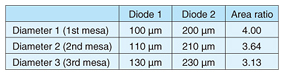
Table 1. Dimensions of large-area diodes.
The C-V curves of two diodes are shown in Fig. 3(a). The capacitance ratio versus bias voltage calculated by two C-V curves is shown in Fig. 3(b). The curve has three steps corresponding to the ratios of the three area sizes of the triple-mesa structure. Since the breakdown voltage of this sample is 27.4 V, these results show that the electric field is confined by the first mesa at the operating condition of M = 10.
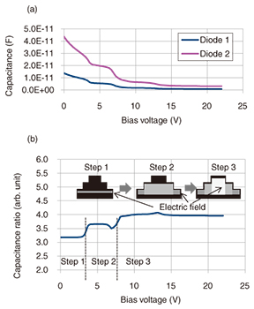
Fig. 3. (a) Capacitance vs. bias voltage curves of two diodes and (b) capacitance ratio vs. bias voltage.
The photocurrent distribution across the APD mesa at a bias condition providing an M value of 10 is shown in Fig. 4. Light was irradiated from the substrate side, and the optical power was set to –20 dBm. The photocurrent curve has a maximum level from –5 to 5 µm due to reflection from the mirror on the top of the first mesa and the high intensity of the electric field under the first mesa, as mentioned above. The 3-dB-down bandwidth was obtained by measuring the OE (opto-electronic) response at the corresponding point. The measured 3-dB-down bandwidth maintains almost the same value in the first mesa and falls off rapidly toward the outside. This indicates that the electric field is sufficiently high only under the first mesa. These results again demonstrate sufficient confinement of the electric field by the first mesa. The 3-dB-down bandwidth at the center reaches 18 GHz even for an M value of 10. This value is sufficient for 25-Gbit/s applications.
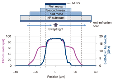
Fig. 4. Cross-sectional profile of photocurrent and 3-dB-down bandwidth against the position of irradiated light.
3. APD-ROSA module for 100-Gbit/s Ethernet systems
Next, we applied our high-speed APD chip to the APD-ROSA. A photograph and schematic illustrations of our 4-ch APD-ROSA are shown in Fig. 5. The size of the package body, excluding the LC-type receptacle and FPCs (flexible-printed circuits), is 7.7 × 20 × 5.8 mm. The APD-ROSA includes a monolithic 4-ch APD array, a planar lightwave circuit demultiplexer (PLC demux), a microlens array, and a commercially available 4-ch transimpedance amplifier (TIA) [9, 10]. Our fabricated silica PLC demux has one single-mode input waveguide and four multimode output waveguides, which provide a flat-top spectrum [11]. The APD-array chip was flip-chip mounted on a subcarrier having signal lines for right-angle surface mounting. Since the glass microlens array and APD array on the subcarrier were attached to the output end of the PLC demux chip, the optical coupling distance between the PLC and APD was minimized to a few hundred micrometers.
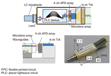
Fig. 5. Schematic view and photograph of 4-ch APD-ROSA.
We measured the back-to-back transmission and the transmission over a 50-km-long single-mode fiber (SMF). The experimental setup is shown in Fig. 6. Here, a 25.78-Gbit/s NRZ (non-return-to-zero) on-off keying optical signal consisting of a 231-1 PRBS (pseudo-random bit sequence) was generated using a tunable laser source and a LiNbO3 Mach-Zehnder (LN) modulator. Wavelengths were set at 1295.56 (lane 0), 1300.05 (lane 1), 1304.58 (lane 2), and 1309.14 nm (lane 3).
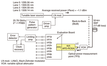
Fig. 6. Experimental setup.
Eye diagrams of the electrical output from the APD-ROSA for back-to-back transmission and after 50-km transmission are shown in Fig. 7(a). We obtained clear eye openings for each lane and for both types of transmission. The BER (bit error rate) characteristics are shown in Fig. 7(b), where the back-to-back receiver sensitivity levels were –20.0, –20.3, –20.1, and –20.0 dBm for lanes 0, 1, 2, and 3, respectively. After 50-km transmission, no significant transmission penalties were observed. Negative values of power penalties are explained by the relationship between the positive chirp parameter of the modulator and the normal chromatic dispersion of the 50-km SMF. These results show that our high-speed APD is applicable to APD-ROSAs for 100-Gbit/s systems, and they also indicate the possibility of extending the transmission distance without increasing the power consumption or package size of the receiver module. The APD-ROSA consumes as little as 0.7 W of power and needs no additional space for a preamp. This configuration opens up the possibility of mounting the ROSA in a CFP4 package and of using it in larger capacity Ethernet systems of the future, such as 400-Gbit/s and 1-Tbit/s Ethernet.
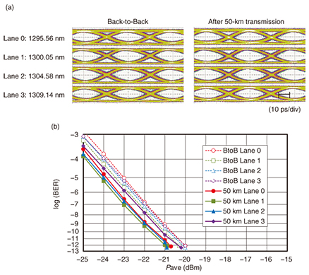
Fig. 7. (a) Electrical output waveforms and (b) BER curves for back-to-back and after 50-km transmission.
4. Conclusion
We developed an inverted p-down APD with high-speed and stable performance. High responsivity (0.9 A/W), large bandwidth (18 GHz at M = 10), and a large GBP (235 GHz) were achieved by optimally designing the absorption layer (1.0 µm) and InAlAs avalanche layer (0.1 µm). The C-V characteristics and photocurrent profile indicate strong confinement of a high electric field in the avalanche layer, which is achieved with two field control layers and a triple-mesa structure.
A 100-Gbit/s (4 × 25-Gbit/s) ROSA using a monolithic four-channel APD array and an ultrasmall PLC demux exhibit minimum receiver sensitivities of –20 dBm and below for back-to-back transmission. We succeeded in achieving 50-km error-free transmission without an optical amplifier. These results indicate that our receiver module technology can contribute to reducing the size and power consumption of optical transceivers toward future 400-Gbit/s and 1-Tbit/s Ethernet multi-wavelength networks.
References
| [1] | IEEE P802.3bs 400 Gb/s Ethernet Task Force,
http://www.ieee802.org/3/bs/ |
|---|---|
| [2] | M. Nada, Y. Muramoto, H. Yokoyama, N. Shigekawa, T. Ishibashi, and S. Kodama, “Inverted InAlAs/InGaAs Avalanche Photodiode with Low-high-low Electric Field Profile,” Jpn. J. Appl. Phys., Vol. 51, No. 2, p. 02BG03, 2012. |
| [3] | M. Nada, Y. Muramoto, H. Yokoyama, T. Ishibashi, and S. Kodama, “InAlAs APD with High Multiplied Responsivity-bandwidth Product (MR-bandwidth product) of 168 A/W·GHz for 25 Gbit/s High-speed Operations,” Electron. Lett., Vol. 48, No. 7, pp. 397–399, 2012. |
| [4] | Y. Muramoto and T. Ishibashi, “InP/InGaAs Pin Photodiode Structure Maximising Bandwidth and Efficiency,” Electron. Lett., Vol. 39, No. 24, pp. 1749–1750, 2003. |
| [5] | J. C. Campbell, “Recent Advances in Telecommunications Avalanche Photodiodes,” J. Lightw. Technol., Vol. 25, No. 1, pp. 109–121, 2007. |
| [6] | E. Yagyu, E. Ishimura, M. Nakaji, S. Ihara, Y. Mikami, H. Itamoto, T. Aoyagi, K. Yoshiara, and Y. Tokuda, “Design and Characteristics of Guardring-free Planar AlInAs Avalanche Photodiodes,” J. Lightw. Technol., Vol. 27, No. 8, pp. 1011–1017, 2009. |
| [7] | Y. Hirota, Y. Muramoto, T. Takeshita, T. Ito, H. Ito, S. Ando, and T. Ishibashi, “Reliable non-Zn-diffused InP/InGaAs Avalanche Photodiode with Buried n-InP Layer Operated by Electron Injection Mode,” Electron. Lett., Vol. 40, No. 21, pp. 1378–1379, 2004. |
| [8] | M. Nada, Y. Muramoto, H. Yokoyama, T. Ishibashi, and H. Matsuzaki, “Triple-mesa Avalanche Photodiode with Inverted P-Down Structure for Reliability and Stability,” J. Lightw. Technol., Vol. 32, No. 8, pp. 1543–1548, 2014. |
| [9] | T. Yoshimatsu, M. Nada, M. Oguma, H. Yokoyama, T. Ohno, Y. Doi, I. Ogawa, and E. Yoshida, “Compact and High-sensitivity 100-Gb/s (4 × 25 Gb/s) APD-ROSA with a LAN-WDM PLC Demultiplexer,” Proc. of ECOC 2012 (38th European Conference and Exhibition on Optical Communication), Th.3.B.5, Amsterdam, The Netherlands, Sept. 2012. |
| [10] | T. Yoshimatsu, M. Nada, M. Oguma, H. Yokoyama, T. Ohno, Y. Doi, I. Ogawa, H. Takahashi, and E. Yoshida, “Compact and High-sensitivity 100-Gb/s (4 × 25Gb/s) APD-ROSA with a LAN-WDM PLC Demultiplexer,” Opt. Express., Vol. 20, No. 26, pp. B393–B398, 2012. |
| [11] | Y. Doi, M. Oguma, M. Ito, I. Ogawa, T. Yoshimatsu, T. Ohno, E. Yoshida, and H. Takahashi, “Compact ROSA for 100-Gb/s (4 × 25 Gb/s) Ethernet with a PLC-based AWG Demultiplexer,” Proc. of OFC (Optical Fiber Communication Conference) 2013, NW1J.5, Anaheim, CA, USA, Mar. 2013. |