|
|||||||||||||
|
|
|||||||||||||
       |
Feature Articles: Photonics-electronics Convergence Hardware Technology for Maximizing Network Performance Vol. 14, No. 1, pp. 25–30, Jan. 2016. https://doi.org/10.53829/ntr201601fa3 Advances in Phase Sensitive Amplifiers Based on PPLN Waveguides for Optical CommunicationAbstractDrastic improvement of the signal-to-noise ratio (SNR) of optical communication systems is necessary in order to make rapid progress in digital-coherent optical communication technology based on multilevel modulated signals. In this article, we describe the recent progress made in phase sensitive amplifiers (PSAs) based on PPLN (periodically-poled lithium niobate) waveguides. These PSAs are capable of low-noise amplification and both phase and amplitude regeneration, which improves the SNR in optical transport systems. Keywords: nonlinear optics, optical parametric amplification, optical signal processing
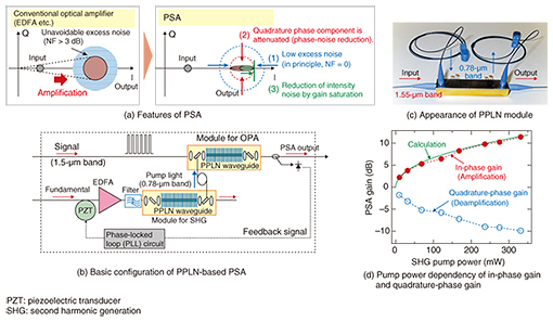
1. IntroductionThe capacity of optical communication systems has been increased in recent years by the improved frequency utilization efficiency achieved with advanced digital-coherent technologies. According to Shannon’s theory, a higher signal-to-noise ratio (SNR) of the signal will be required to achieve a higher frequency utilization efficiency of the system. However, the achievable transmission distance and channel capacity are now approaching their limits due to the degradation of the SNR by the accumulation of noise from repeater optical amplifiers and inter-symbol interference caused by nonlinear impairments in the transmission optical fiber [1]. Therefore, a drastic improvement in the SNR is necessary for future optical communication systems. 2. PSA using highly efficient PPLN waveguidesA signal-phase-dependent amplification characteristic can be achieved with optical parametric amplification (OPA), which transfers the energy of an intense pump light to the signal light. It amplifies the in-phase component of a signal relative to the phase of the pump and de-amplifies the quadrature component. This phase sensitivity makes it possible to provide several unique features of the phase sensitive amplifier (PSA). The key feature is that the ideal noise figure (NF) of a PSA is 0 dB [2]; in other words, optical amplification without SNR degradation is possible (feature (1) in Fig. 1(a)), whereas the NF of a phase insensitive amplifier (PIA), for example, an erbium-doped fiber amplifier (EDFA), cannot be reduced below the 3-dB quantum limit. Furthermore, a PSA can reduce the phase noise by squeezing the phase because it de-amplifies the quadrature component (feature (2) in Fig. 1(a)). A PSA also provides amplitude regeneration by means of gain saturation thanks to the high-speed response of the parametric process (feature (3) in Fig. 1(a)). Therefore, PSAs are now attracting a great deal of interest for use in enhancing the SNR of inline optical repeater systems because of their potential for low noise amplification and their signal regeneration capabilities. The basic setup for our recent experimental work on periodically-poled lithium niobate (LiNbO3) (PPLN)-based PSAs is shown in Fig. 1(b). Two PPLN waveguides were used for second harmonic (SH) pump generation and OPA, respectively. High conversion efficiency and high power tolerance are both desirable in order to achieve a high parametric gain. We developed PPLN ridge waveguides using the direct bonding method, which made the waveguides highly resistant to photorefractive damage [3]. We used the dry etching technique to obtain a ridge waveguide with fine uniformity, which yielded high SH conversion efficiency. Recent advances in PPLN waveguides and related module packaging technology have enabled us to explore χ(2)-based PSAs for optical communication [4]. The PPLN waveguides were assembled into fiber-pigtail modules. The modules have four input/output ports to allow SH pumping. To achieve a stable PSA output, an optical phase-locked loop (PLL) is used to compensate for the slow relative phase drifts between the signal and SH-pump lights. A photo of the module is shown in Fig. 1(c). Polarization-maintaining fibers for 1.55 and 0.78 μm were respectively used in the two signal ports and the two pump ports. The signal and SH pump were combined with a dichromatic mirror and injected into the waveguide inside the module. The module packaging technology enabled us to achieve both low insertion loss and stable operation. The in-phase gain and quadrature-phase gain as a function of the SH pump power is shown in Fig. 1(d). By increasing the SH pump power, the in-phase gain was increased and the quadrature-phase gain was decreased symmetrically. A gain over 10 dB was obtained, and the pump power dependence agreed well with the theoretical curve. Nearly perfect phase sensitive amplification characteristics were obtained because the ridge waveguide provides a sufficient spatial mode overlap between the signal and SH pump light, and temporal mismatching is prevented thanks to continuous wave pumping.
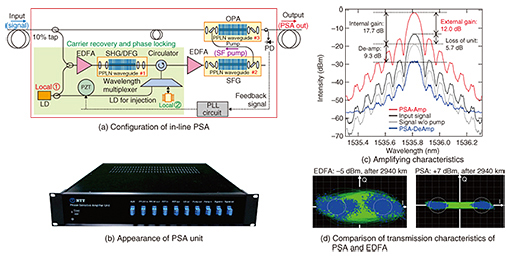
Probably the most intriguing property of a PSA is the ‘0 dB’ quantum-limited NF. We evaluated the NF of a degenerate PSA, where the signal and an idler were the same wavelength. We confirmed the low noise characteristics in which the NF values of the PSA were 1.8 dB, which is below the standard quantum limit of 3 dB, by using an optical and an electrical spectrum analyzer [5]. We believe the measured NF was largely due to the extrinsic coupling loss; therefore, the intrinsic NF was very close to 0 dB. 3. Multi-repeater transmission using amplitude and phase regeneration by in-line PSAIn addition to its capacity for low NF amplification, a PSA has a phase and amplitude regeneration capability that is achieved by using the phase squeezing property and by operating the amplifier in the saturated regime. These capabilities mean that PSAs will have a large impact on long-haul transmission if they are used as multiple repeaters. For the repeater operation of the PSA, the phase of the pump should be locked to that of the input signal. The configuration of an in-line PSA for a binary phase shift keying (BPSK) signal using a carrier-recovery and phase-locking system is shown in Fig. 2(a). The tapped signal is converted to SH light in the PPLN waveguide. Doubling the signal phase makes it possible to recover the carrier from a BPSK signal without a carrier component. The carrier phase is copied to the 1.5-μm-band idler wave by the difference-frequency generation (DFG) process. Then the recovered carrier phase is locked by injecting the idler into a local laser. The in-line PSA, which operates as a repeater amplifier, is achieved using the phase-locked local light. The key components in Fig. 2(a), including the three PPLN modules, an LD (laser diode) for injection, and a PZT (piezoelectric transducer) for the PLL, were assembled into a PSA unit as shown in Fig. 2(b) to obtain stable operation. We obtained a high external gain of 12 dB for a BPSK signal using the in-line PSA as shown in Fig. 2(c). We also examined the regeneration capability of the in-line PSA in a multi-span transmission. A comparison of the transmission performance for both the PSA and an EDFA at the same link is shown in Fig. 2(d). The left constellation is for the EDFA link after about 3000-km transmission in an optimal power condition. The signal quality was degraded by amplified spontaneous emission (ASE) noise and fiber nonlinearity. However, thanks to the phase and amplitude regeneration capabilities of the PSA, the inter-symbol interference caused by the phase noise resulting from fiber nonlinearity and the intensity noise caused by the ASE of an optical amplifier are largely suppressed, as shown in the right constellation.
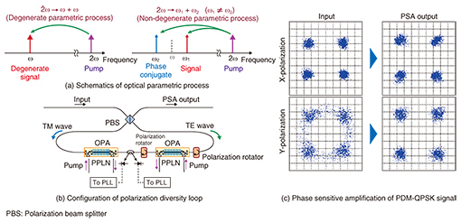
4. PSA for multilevel phase coded and polarization-division multiplexed signalThe in-line PSA using degenerate parametric amplification mentioned above can only handle a binary modulated signal. The high capacity communication of the future will most likely operate with spectral efficiencies greater than 1 bit/s/Hz, thereby requiring the use of multilevel phase coding and polarization-division multiplexing. Extending the applicability to a polarization-division multiplexed (PDM)-QAM (quadrature amplitude modulation) signal is practically very important in order to install the PSA in a practical system based on digital-coherent technologies. For the OPA process, energy is transferred from a pump light with a frequency of 2ω to a signal light and an idler light with frequencies of ω1 and ω2. When ω1 = ω2, the process is said to be degenerate, and when ω1 ≠ ω2, the process is said to be non-degenerate (see Fig. 3(a)). For the non-degenerate process, a multilevel-modulation signal can be handled by using a phase conjugate signal as the idler. Moreover, a polarization diversity scheme is required to handle the PDM signal because a second-order nonlinear optical medium such as PPLN is usually polarization dependent. A schematic view of the proposed polarization diversity loop configuration is shown in Fig. 3(b). In this setup, the two waveguides are arranged in series, and a rotator is installed between them. The configuration combines the advantages of being free of delay alignment and having low reflection noise. Although the loop configuration was used to achieve polarization diversity without any delay adjustment, the TM (transverse magnetic) and TE (transverse electric) waves are independently amplified by two different waveguides. The capability of amplification for multilevel-modulated and PDM signals was confirmed by using the non-degenerate process and the diversity configuration. The transmitter generated a 20-Gbaud quadrature phase shift keying (QPSK) signal, and a phase-conjugated idler was generated by DFG. After the DFG process, a PDM emulator was used to generate an 80-Gbit/s PDM-QPSK signal with a phase conjugated idler. A LiNbO3 phase modulator was used to add phase noise to confirm the phase regeneration capability of the PSA. Constellation diagrams for an 80-Gbit/s PDM-QPSK input signal with phase noise and the output signal after using the PSA are shown in Fig. 3(c). The constellation for the Y-polarization of the input signal indicates that larger phase noise was induced than that for the X-polarization because of the polarization dependence of the LiNbO3 phase modulator. The constellation points were rotationally spread due to the large phase noise. After using the PSA, a major phase noise reduction was achieved with the canceling effect. The phase sensitive amplification of the PDM-QPSK signal was confirmed from the inherent noise canceling characteristics of the PSA.
5. ConclusionWe introduced PSAs based on PPLN waveguides that have capabilities of low noise amplification and both phase and amplitude regeneration for improving the SNR in optical transport systems. We will contribute to further expanding the capacity of future backbone optical communication systems by maximizing the potential of digital-coherent technologies. Part of this research uses the results of “R&D on Optical Signal Transmission and Amplification with Frequency/Phase Precisely Controlled Carrier” commissioned by the National Institute of Information and Communications Technology of Japan. References
|
||||||||||||