|
|||||
|
|
|||||
       |
Front-line Researchers Vol. 14, No. 1, pp. 6–11, Jan. 2016. https://doi.org/10.53829/ntr201601fr1  Making Photonic Devices Dramatically Larger in Scale and Lower in PriceOverviewShinji Matsuo, Senior Distinguished Researcher at NTT Device Technology Laboratories, continues his challenging work on achieving optoelectronic integrated circuits on silicon substrates and making them into economical and low-power devices—key issues in the worldwide information technology industry. He leads a group dealing with a unique form of research, so we asked him to give us some background on the inception of this groundbreaking technology. We also asked him to describe remaining issues and to comment on his role as a researcher. Keywords: photonic device, optoelectronic integrated circuit, laser on Si
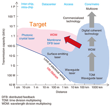
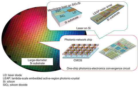
Laser on Si: a long-standing challenge—Dr. Matsuo, please tell us about your current research efforts. In Japan, mobile data traffic is predicted to grow by about 1000 times the 2010 level by 2025. At datacenters too, traffic volumes are growing at an amazing rate. Facility investment is needed to deal with this jump in traffic, but passing on this cost to customers through usage fees must be prevented. The amount of power used by datacenters is also a key issue. In the United States, for example, it accounts for a substantial percentage of all power consumed in the country. In this regard, 70% of datacenter traffic is made up of communications within the datacenter, so “economical” and “low-power” are becoming important keywords when talking about short-range optical communications in datacenters. In photonic devices too—my field of research—there is considerable activity in solving these problems in optical communications. In the field of electronic devices such as silicon-based complementary metal-oxide semiconductors (CMOS), innovation in integration technology has enabled the number of transistors in an integrated circuit to increase by 1 million times over a 40-year period in accordance with Moore’s law while minimizing cost increases. In the field of photonic devices, however, the modularization of individual components such as lasers, light-receiving elements, and isolators is still just a concept. To achieve photonic devices with large-scale integration and low cost on a level equivalent to that of electronic devices, we need to develop optoelectronic integrated circuits on a silicon platform and establish silicon photonics technology that can increase integration density by 100–1000 times that of current levels. To this end, we have been looking into the use of compound semiconductors such as indium phosphide (InP) and gallium arsenide (GaAs) in the field of optoelectronic integration in a scheme similar to the use of silicon. If this could be achieved and if semiconductor lasers could be manufactured by a mechanism similar to that of a silicon fab*, the cost per bit could be decreased by 1/1000 in 20 years by what we could call an optical version of Moore’s law (Figs. 1–3).
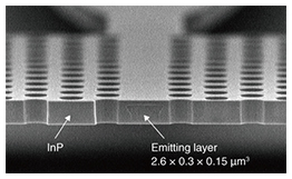
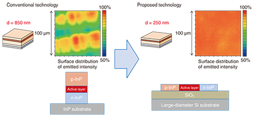
—Has this research progressed smoothly? There are two main technical issues in achieving laser on Si (silicon). These have presented a challenge to me ever since I entered NTT laboratories about 30 years ago. The first is lattice misalignment. The atomic size of silicon (group IV in the periodic table) and that of compound semiconductors such as InP and GaAs (group III-V) are different, so growing a compound semiconductor directly on silicon is extremely difficult. To resolve this issue, we developed technology for preparing silicon and a compound semiconductor separately and then joining them directly at the atomic level. The other issue is different thermal expansion coefficients. The temperature in the laser fabrication process increases from room temperature to 600°C, but the thermal expansion coefficients of silicon and InP differ greatly. As a result, the different amount of thermal expansion in those materials as the process temperature changes can cause strain and stress to occur, which can lead to defects in the crystal and a significant drop in device characteristics. In light of this, conventional semiconductor lasers have been fabricated with a thickness of several micrometers. However, by making use of membrane lateral injection fabrication technology developed in conjunction with a LEAP (lambda-scale embedded active-region photonic-crystal) laser that we successfully developed in 2013, we achieved a breakthrough in laser membrane thickness, reducing it to about 1/10 that of the conventional level. I believe that this achievement was a direct result of the world-class expertise of NTT laboratories in epitaxial growth technology and optical semiconductor processing technology (Fig. 4).
—What issues lie ahead? I would like to try fabricating an actual large-scale photonic integrated circuit with lasers using a silicon fab. Of course, the use of a silicon fab means that this would not be something that NTT could accomplish on its own, so we would need to do this together with many other parties. To this end, we will promote discussions at international conferences that up to now have not been directly related to lasers and actively pursue joint research with outside parties. We will also work to persuade industry leaders, university professors, etc., to support the direction of our research. —This research has been attracting attention in many countries. What has been the response? I have had many opportunities to present my research in the form of invited lectures in Europe, the United States, China, and other countries to people involved in similar research, so I feel that interest is growing in our technology. I have also noticed a growing interest from other fields in our technology for fabricating lasers on silicon. The questions that I receive have likewise been changing from general impressions such as “very unique characteristics” to specific inquiries such as “Can this really be used?” and “Can this be incorporated in the silicon fab mechanism?” I think this is because of growing expectations for actual application and commercialization of this technology. Thus, while I think that this is a great accomplishment from a technical point of view, there are still issues that need to be resolved in terms of reliability and cost efficiency before we reach a practical stage. This research is progressing steadily, but when considering the objectives to be attained, it is still in its second stage. “You evaluate yourself”—surrounding yourself with brilliant people and recognizing your strong points—In what sort of environment and from what mindset did these epoch-making research achievements originate? We have abundant human resources at NTT laboratories, with specialists in a variety of fields, and I enjoy having the opportunity to chat with such bright people over drinks whenever possible. Our discussions at such sit-downs are lively, and new projects may get off the ground with declarations such as, “If that’s the case, let’s work together and give it a try!” Senior Distinguished Researcher Masaya Notomi, known for his research in photonic crystals, is one such colleague. In the actual research process, ideas may come to such specialists in a variety of ways. Because such a distinguished group of people have been purposely brought together, it’s imperative that ways be found for making the most of their amazing abilities in my research with the ultimate aim of producing results. It was once said to me: “You know best as to who has the technology that we need.” On hearing that, I suddenly realized one of my strong points—knowing where to find certain technologies. I also keep in mind that “you evaluate yourself,” and that I should be careful not to be swayed by the judgments of others. This mindset actually began when I succeeded for the first time in achieving laser oscillation on a silicon substrate. I immediately tried to announce this technology in a post-deadline paper at the Optical Fiber Communication Conference, but the paper was not chosen. However, I persevered in announcing my results in later papers and elsewhere, and I finally began to receive some recognition. In other words, the position, background, viewpoint, etc., of an evaluator can influence the evaluation in question. The same holds true for evaluations within the company. The staff of a company is not solely composed of specialists, so it cannot be said that those evaluations are always correct. For me, in all honesty, you live or die by whether a device works or fails rather than by the opinions of others. I take great pleasure in research. By the way, to tell you something about my personal life, I put a lot of effort in tending the garden at home. Similar to research, flowers may not bloom as expected, and weeds that spring up daily must be constantly pulled. However, unlike research, results in gardening can be obtained relatively quickly, and most people will find the results of your time and effort and care as something beautiful. This is why gardening is relaxing and enjoyable for me. In the case of research, it’s not all praise; most feedback is negative in nature. —As an active researcher, what do you think is important to produce results? I believe that a change in perspective can be very helpful. It is also important to have motivation and to merge information. In 1997, exactly ten years after entering NTT, I was assigned to the NTT laboratory in Yokosuka, where I was given the opportunity to work on optical communications systems for about three years. This was the first time that I had been involved in the development of systems-related technology, since I had researched only components and devices up to then. However, I am still using the mindset and outlook that I developed there in my current research. In addition, just hearing about the situation in the United States with regard to the need to reduce power consumption in optical semiconductor devices—which is being researched there in the form of government-supported projects—has motivated me greatly in my work. In particular, it has helped me to see the importance and significance of this research. I have been invited to a variety of international conferences in recent years, and ideas sometimes come to me from things that I hear at those events. At such times, I promptly email my colleagues or young researchers in Japan involved in photonic device research. I am motivated not just by discussions with specialists but by a variety of things including social phenomena. I have a constant desire to create something new by combining such ideas with technology that I am already knowledgeable about. In a senior position, however, I must take on more management activities, which limits the time that I can allocate to real research. I therefore have the responsibility to consider the extent to which I myself should contribute to this research and how I should navigate the researchers under me in the right direction. Nevertheless, I think that it is very important for me as an active researcher to be at the forefront of this research. I would not be able to judge what is crucial just listening to other people and not doing my own research. If I were to lose my edge here, I would not, in the end, be able to use my research time efficiently, and I would not know how to merge all the information I was taking in. However, being too absorbed in my own research would prevent me from receiving information from those around me or leave me with no time for management tasks. Thus, it is important that I strike a balance between what I should do myself and what I should entrust to others. Establishing one’s core is essential to a researcher—By the way, why do you continue to be an active researcher? In my younger days, I experienced what it felt like to be completely absorbed in research. Some things can only be understood after making many attempts to solve a problem. This experience involved not only work on intricate and critical problems but everyday failures and mishaps as well. Looking back, I can now laugh at this incident, but once when trying to observe a wafer with a microscope, I accidently damaged the wafer when adjusting the microscope’s height. Even science textbooks in elementary school describe the proper way of using a microscope. This simple event demonstrates that sometimes there are things that one should know how to do but can’t. Doing even a simple task repeatedly can enhance one’s power of judgment and enable one to better understand cause-and-effect relationships or other phenomena based on experience. I feel that the sense of “this is just what is needed” is backed by experience and that one should first become adept at any task you are called to do. There has recently been talk about the need for researchers to gain experience in other fields such as business or sales to broaden their perspective. However, I would like to have researchers become totally absorbed in their work for about ten years at first to develop their core skills. I think that the number of researchers without such core attributes have been increasing in recent years. If there is no field in which a researcher who has accumulated such a variety of experiences can apply all of them, such experiences have no meaning in the end. —Dr. Matsuo, please leave us with a few words for all of our young researchers. When you first start out as a young researcher, failure is commonplace. But during that time, you will unconsciously be gaining experience as to where to back off and where to devote all your energy. Research is indeterminate, unpredictable work, so no one knows just what the results might be. Please take up the challenge that research presents with all your heart! This also means doing work that you will be responsible for above and beyond your duties as a researcher and employee in an organization, although it’s still okay to be practical about your work and make time for yourself too. In cooking, which is one of my hobbies, you usually don’t fail as long as you follow the recipe. Research, however, is different; there are no set recipes. Therefore, you, the researcher, must add your own creative touch. Do not lose sight of your original objective and path. Even after a string of failures, you should list your daily achievements within that time and enjoy your research to the fullest. ■Interviewee profileShinji MatsuoSenior Distinguished Researcher, Materials and Devices Laboratory of NTT Device Technology Laboratories and NTT Nanophotonics Center. He received a B.E. and M.E. in electrical engineering from Hiroshima University in 1986 and 1988, and a Ph.D. in electronics and applied physics from Tokyo Institute of Technology in 2008. He joined NTT Opto-electronics Laboratories in 1988, where he researched on photonic functional devices using multiple quantum well pin modulators and vertical cavity surface-emitting lasers. In 1997, he researched optical networks using WDM technologies at NTT Network Innovation Laboratories. Since 2000, he has been researching high-speed tunable optical filters and lasers for photonic packet switching at NTT Photonics Laboratories. He is a member of the Institute of Electrical and Electronics Engineers Photonics Society, the Japan Society of Applied Physics, and the Institute of Electronics, Information and Communication Engineers. |
||||