|
|||||||||||||||||||||||||||||||
|
|
|||||||||||||||||||||||||||||||
       |
Regular Articles Vol. 14, No. 4, pp. 54–61, Apr. 2016. https://doi.org/10.53829/ntr201604ra2 Drift Transport of Helical Spin Coherence in SemiconductorsAbstractSpatial transport of electron spins and their electrical manipulation are fundamental technologies in the emerging field of semiconductor spintronics, where the spin degree of freedom is used as an information carrier in a device. Images of the spatial distribution of drifting spins were obtained using Kerr rotation microscopy in a GaAs quantum well where special symmetry of the spin-orbit interaction, namely a persistent spin helix (PSH) condition, was achieved. By efficiently suppressing the spin relaxation in the PSH state, we were able to demonstrate long-distance transport of electron spins over 100 µm and electrical control of the spin precession during drift transport. In a PSH condition, the frequency of the spin precession shows significant anisotropy, reflecting the dependence of effective magnetic fields on crystal orientation. A theoretical model reproduced the spin distributions well and revealed that the spin decay length was maximized near the PSH condition. The robustness of the spin coherence with respect to the variation of transport trajectory was also confirmed by employing a time-dependent in-plane electric field perpendicular to the drift direction. Further development of this technique will advance the field of semiconductor spintronics, including the physics of spin-charge coupled systems as well as applications for future spin devices. Keywords: spintronics, spin-orbit interaction, Kerr rotation
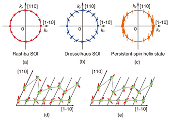
1. IntroductionRecent developments in electronics rely on the miniaturization and integration of electronic devices in which an electron’s charge is used as an information carrier. However, device size is approaching its limit, and device performance cannot be further enhanced simply by extending existing technologies. An emerging research field known as semiconductor spintronics represents an attempt to use spin instead of charge for information processing [1–3], since this will result in lower energy consumption, higher operating speeds, and further improvement of device functionality compared with conventional charge-based devices. The electrical control and transport of electron spins are essential techniques for realizing spintronics devices. An effective magnetic field plays an important role in controlling electron spins by electrical means. In general, the asymmetry of the system (e.g., the asymmetric layer structure of a quantum well (QW) or the lack of an inversion center in crystal structures) generates an internal electric field that is converted into effective magnetic fields for the coordinate system of a moving electron [4]. This is due to a relativistic effect called a spin-orbit interaction (SOI). However, SOI is a double-edged sword with spintronic devices. Because the direction of effective magnetic fields depends on the electron momentum, multiple scattering of electrons randomizes the effective magnetic fields, resulting in undesired spin relaxation [5]. A significant difficulty in the application of electron spins to semiconductor devices is preventing spin relaxation, which limits the transport length of electron spins to the order of 10 µm in semiconductor heterostructures [6]. Currently, much attention is being focused on the suppression of spin relaxation by balancing two SOIs. In III-V semiconductor heterostructures, there are typically two kinds of SOIs. One is the Rashba SOI induced by the internal electric field in an asymmetric QW [7]. The other is the Dresselhaus SOI, which originates from the crystal field induced by the bulk inversion asymmetry in a zinc-blende crystal structure [8]. The Rashba and Dresselhaus SOIs act on electron spins as momentum-dependent magnetic fields as shown in Figs. 1(a) and 1(b). When the strengths of these two SOIs are equal, the effective magnetic field is uniaxially oriented as shown in Fig. 1(c). In this condition, electron spins can precess around the same axis and do not relax even if they experience multiple scattering (Figs. 1(d) and 1(e)). This special condition of SOIs is called the persistent spin helix (PSH) state, which has been theoretically predicted and experimentally confirmed [9–11]. In the PSH state, the spin transport length can be enhanced even in a system with strong SOIs.
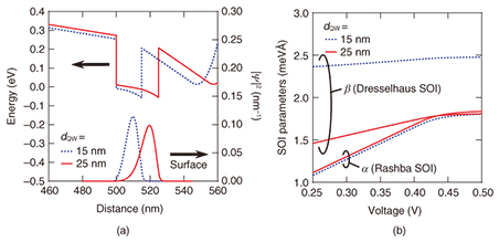
Here, we report the spatial mapping of drifting spins in a GaAs QW where the Rashba and Dresselhaus SOIs are balanced to achieve a PSH state [12]. In the PSH state, the precession frequency of drifting spins becomes anisotropic, reflecting the crystal orientation dependence of the effective magnetic field. A comparison of experimental results and a numerical simulation based on a spin-drift diffusion model reveals that the spin decay length is maximized near the PSH condition, indicating the effective suppression of spin relaxation by the PSH state. Within the enhanced distance of the spin transport, the transport path of electron spins can be modulated by employing time-varying in-plane voltages, suggesting the robustness of the spin coherence against geometrical variations in the spin transport. 2. ExperimentTo determine a suitable structure for the PSH condition, we calculated the SOIs in a GaAs single QW structure. The Hamiltonians for the Rashba and Dresselhaus SOIs in a III-V semiconductor QW are given by where α and β indicate the strengths of the SOIs, σi(i = x, y) is the Pauli matrix, and ki(i = x, y) is the electron momentum. In this article, we defined the coordinate axis with base vectors x || [1-10], y || [110], and z || [001]. Since the potential gradient in a QW can be modulated with an external gate voltage, the Rashba SOI parameter α is a gate-controllable value. In contrast, β is expressed by material constant γ and well thickness d in the following equation, According to Eq. (3), the Dresselhaus SOI is enhanced by reducing the well thickness. By solving the Poisson-Schrödinger equation, we can calculate energy band profiles and wave functions in the AlGaAs/GaAs/AlGaAs QW structures, as shown in Fig. 2(a). To confirm the contribution of the Dresselhaus SOI, we assumed two different QW thicknesses of d = 15 and 25 nm. The gate-voltage dependences of SOI parameters calculated by using k·p perturbation are shown in Fig. 2(b) [13]. It should be noted that the horizontal axis in Fig. 2(b) indicates the relative difference between the potentials of the surface and the substrate, which does not correspond to the experimentally applied gate voltage. In Fig. 2(b), we found that the Dresselhaus SOI parameter β depends strongly on the well thickness, whereas the Rashba SOI parameter α can be widely modulated by applying a gate voltage rather than by varying the well thickness. According to Fig. 2(b), α can be comparable to β in a 25-nm-thick QW, which indicates the possibility of the PSH condition.
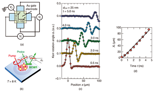
Using the theoretical calculations as a basis, we designed and grew 15- and 25-nm-thick modulation-doped Al0.3Ga0.7As/GaAs/Al0.3Ga0.7As single QW structures by molecular-beam epitaxy on a (001) semi-insulating GaAs substrate. The QWs were located 120 nm below the surface, and three δ-doping layers were embedded 50, 100, and 105 nm below the surface. The epitaxial wafers were fabricated into cross-shaped structures with four ohmic contacts consisting of AuGeNi layers. The central part of the structure was covered with a semi-transparent Au gate electrode as indicated in Fig. 3(a). We employed Kerr microscopy to measure the spin dynamics of the drifting electrons (Fig. 3(b)). Spin-polarized electrons were generated by a circularly polarized pump light. Subsequently, the spatial distribution and dynamics of the electron spins were detected with a linearly polarized probe light via the Kerr rotation angle θK, which was proportional to the spin density at the focused position. For a microscopic measurement of the spin coherence, the pump and probe lights were focused on the sample with 6-µm- and 3-µm-diameter spots, respectively. The temporal development of the electron spins can be observed by using a pulse laser from a mode-locked Ti:sapphire laser, whereas the steady flow of drifting spins can be measured with a continuous wave (CW) laser. All the measurements were carried out at 8 K. 3. Results and discussionThe results of time-resolved Kerr rotation microscopy for the drifting spin in a 25-nm-thick QW with the application of an in-plane electric field Vx = 200 mV are shown in Fig. 3(c). We can see that spin-polarized electrons generated at time t = 0 ns move to the drain electrode. Even in the absence of an external magnetic field, we observed a spin precession resulting from the effective magnetic field induced by the SOIs. To estimate the drift velocity of the electron spins, we performed a fitting analysis on the assumption that the spatiotemporal development of drifting spins can be explained by the model function, where A is the signal amplitude, x0 and w are the displacement and width of the Gaussian, respectively, and kSO is a spin wavenumber that represents the spatial frequency of the spin precession. We fitted Eq. (4) to the experimental result and extracted x0, which is plotted as a function of time in Fig. 3(d). We found that x0 is proportional to time t, and the slope in Fig. 3(d) indicates the drift velocity. Thus we obtained vd = 20.6 km/s in a 25-nm-thick QW, which is 150 times faster than the drift velocity of the electron spins observed in bulk GaAs [14].
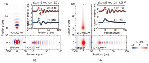
The spatial distribution of drifting spins in a steady state is shown in Figs. 4(a) and 4(b). In a 15-nm-thick QW, spin precession due to the effective magnetic field was observed in both the x and y directions, which reflects the isotropic strength of the effective magnetic fields. This is because the Dresselhaus SOI is dominant in the 15-nm-thick QW as predicted by a theoretical calculation. In contrast, in a 25-nm-thick QW when Vg = –4.28 V is applied, the precession of the drifting spins in the y direction is stopped completely, although drifting spins in the x direction precess more than five cycles in 100 µm. This strong anisotropy of the spin precession originates from the dependence of the effective magnetic field on the crystal orientation, which implies that the PSH is almost realized in a 25-nm-thick QW. Furthermore, the long-distance spin transport over 100 µm observed in the 25-nm-thick QW is attributed to the suppression of spin relaxation due to the PSH state. To determine quantitatively how close this was to the PSH condition, we performed a fitting analysis of the spatial distributions of the drifting spins. On the assumption that the contribution of the drift transport of the spins is dominant compared with spin diffusion, the spatial variation of the spin flows is given by, where d is the distance from the origin and λSO is the spin decay length. We fitted Eq. (5) to the experimental results and extracted the spin wavenumber kSO. We excluded data between d = 0 µm and 10 µm from the fitting procedure to remove the contribution of spin diffusion. If we assume simple one-dimensional transport, the SOI parameters are proportional to the spin wavenumber, 
where m* and ћ are the effective mass of an electron and Planck’s constant, respectively. Thus, two SOI parameters, α and β, can be estimated from kSO in the [1-10] and [110] directions. The estimated SOI parameters were α = 0.58 meVÅ and β = 2.10 meVÅ for a 15-nm-thick QW and α = β = 0.99 meVÅ for a 25-nm-thick QW. From these results, we confirmed that the PSH state is realized in a 25-nm-thick QW.
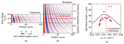
The spatial frequency of the spin precession during drift transport is electrically controlled by the gate modulation of the Rashba SOI. The gate voltage (Vg) dependence of θK scanned along the [1-10] direction for Vx = 50 mV and Vy = 0 mV is shown in Fig. 5(a). By varying the gate voltage, we were able to continuously modulate the spatial frequency of the drifting spin precession via gate control of the Rashba SOI. This behavior was well reproduced by a simulation based on a spin-drift-diffusion model, as shown in Fig. 5(b). Assuming that the precession period in Fig. 5(a) depends only on α, we can compare the effect of α on the transport length by plotting spin decay length λSO versus spin wavenumber kSO, where both parameters can be extracted by the fitting procedure used in Fig. 4. The obtained λSO values are plotted as a function of kSO in Fig. 5(c). In both the experiment and the simulation, λSO decreases as kSO diverges from the balanced condition α = β, indicating that the suppression of the D’yakonov-Perel spin relaxation caused by the PSH also appears in the spin transport length.
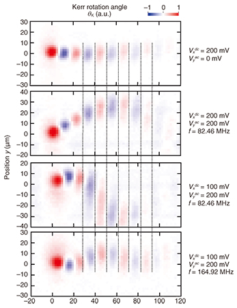
We can transport the helical spin state along arbitrary trajectories by using a time-dependent in-plane electric field. We applied a sinusoidal ac voltage Vyac with frequency f in the y direction and dc voltages Vxdc in the x direction. To excite spins at the timing of a certain phase of Vyac, the initial spins were excited with a pulsed pump light from a mode-locked laser whose repetition frequency was synchronized with f or f/2, whereas the Kerr signal was detected with a probe light from a CW laser. When a sinusoidal voltage was applied in a transverse direction to the drift spin transport, a clear spin flow along a winding path was observed (Fig. 6). The stripe patterns in the spin packet are maintained regardless of the transport trajectories. This is because in a PSH condition, spins always precess in an x-z plane, and the precession phase depends only on x [9, 10]. For all transport paths, the spin phase was conserved even at distances much longer than the precession periods, and thus, the technique will be beneficial for further exploitation of the SOI in drift spin manipulation.
4. ConclusionThe spatial distribution of drifting spins in a GaAs QW where two types of SOI, namely the Rashba and Dresselhaus SOIs, are balanced to realize a PSH state, was mapped by using temporally and spatially resolved Kerr rotation microscopy. In the PSH state, spins drifting in a direction where there are strong effective magnetic fields exhibit a fast spin precession, whereas the spin precession of spins drifting in an orthogonal direction is completely stopped. The spin decay length is maximized near the PSH condition, indicating the effective suppression of spin relaxation by the PSH state. Furthermore, we demonstrated drift spin transport over 100 µm, where the precession frequency was controlled by an external gate voltage. The results presented here show that spin coherence with a balanced SOI can be efficiently transferred to a distant place. We confirmed the robustness of the spin phase for the variation of transport paths in the PSH state. If the PSH condition is sufficiently maintained, we may also manipulate the spin states by using the gate bias voltage or a trajectory-controlled quantum operation. Further development of this technique will advance the field of semiconductor spintronics, including the physics of spin-charge coupled systems as well as applications for future spin devices. AcknowledgmentsWe thank P. V. Santos of Paul-Drude-Institut für Festkörperelektronik, Berlin, Germany, and J. Nitta and M. Kohda of the Department of Materials Science, Tohoku University, Sendai, for their useful technical advice. This work was partly supported by the Japan Society for the Promotion of Science (JSPS). References
|
||||||||||||||||||||||||||||||