|
|||||||||||||||||||||||
|
|
|||||||||||||||||||||||
       |
Feature Articles: Device Technology Development for Beyond 100G Optical Transport Network Vol. 14, No. 9, pp. 6–12, Sept. 2016. https://doi.org/10.53829/ntr201609fa2 Digital Signal Processor (DSP) for Beyond 100G Optical TransportAbstractAs a foundation for the coming full-fledged big data society, optical communication networks must further advance in speed, capacity, and cost-effectiveness. This article introduces beyond 100G (beyond 100 Gbit/s per channel) digital coherent optical transmission technology, which is a key to developing high-capacity optical communication networks, and the digital signal processor (DSP) that provides core functions for this technology. Keywords: digital coherent optical transmission, digital signal processing, multi-level modulation scheme
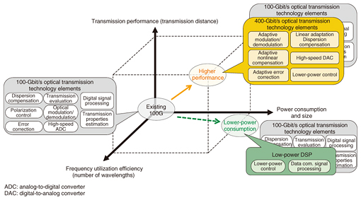
1. IntroductionRecent advances in telecommunications technology are expected to usher in a full-fledged big data society. These advances include the spread of FTTH (fiber to the home), the growing use of smartphones, the development of the 5G (fifth-generation) mobile communication system, which provides super-high-speed mobile access, and the introduction of the IoT (Internet of Things), in which everything is interconnected via the Internet. This trend demands that we achieve further advances in the speed, capacity, and cost-effectiveness of optical communication networks, as they are the foundation for many communication services. One technology that is expected to satisfy this demand and that has been gaining attention in recent years is digital coherent optical transmission. This uses coherent detection to improve both receiving sensitivity and frequency utilization and employs digital signal processing to achieve compensation for waveform distortion, which accumulates in long-distance optical fiber transmission [1, 2]. Such waveform distortion compensation has so far been difficult to achieve. Digital coherent optical transmission technology is already used in high-capacity transmission systems that operate at a level of 100 Gbit/s per channel. With this technology, wavelength-division multiplexing (WDM) optical transmission systems with a total capacity of 8 Tbit/s have been introduced commercially. Currently, the standardization of 400-Gbit/s Ethernet transmission is in progress. This provides the potential for commercial development of beyond 100-Gbit/s per channel (beyond 100G) optical transport technology. The trends in the development of digital signal processing technology for digital coherent optical transmission are shown in Fig. 1. There are two possible directions for improving the technology applied to the existing 100-Gbit/s transmission: enhancing performance and reducing power consumption. A high performance digital signal processor (DSP) needs to increase in both transmission capacity and distance with realistic power consumption to be implemented in transmission equipment. In contrast, a low-power DSP requires low-power consumption, a small package size, and low cost for implementation with metro-access and datacenter networks.
This article focuses on the former, in particular, on extending the distance of beyond 100G transmission. To increase the transmission capacity per fiber, it is necessary to enhance frequency utilization. An effective way to achieve this is to increase the number of modulation levels in the optical amplitude and/or phase. However, if the number of modulation levels is to be increased, the optical signal-to-noise ratio (OSNR) required to achieve the desired symbol error rate also needs to rise. If the transmission power is increased to raise the OSNR, inter-symbol interference caused by the nonlinear optical effects of the optical fiber increases, which in turn reduces the possible transmission distance. Therefore, if we are to implement a beyond 100G optical transport system, we need to combine a number of technologies, including nonlinear compensation technology, which compensates for nonlinear optical effects, and high coding gain FEC (forward error correction). In addition, we have to consider applying adaptive modulation/demodulation technology, which adaptively selects the modulation/demodulation method most suitable for the particular transmission performance margin in order to maximize the network transmission capacity. Another effective way to increase frequency utilization is to reduce the frequency spacing between adjacent channels in WDM. This requires the frequency spectrum of the optical signal to be narrowed. Nyquist filtering is essential for this because it enables digital signal processing at the transmitter to narrow the optical signal spectrum with minimum degradation in signal quality. To develop a beyond 100G optical transport system, it is important to achieve these signal processing functions with a practical level of power consumption. 2. Digital coherent optical transmission technologyAn overview of the digital coherent optical transmission technology is shown in Fig. 2. The modulation method most commonly used in conventional optical transmission systems has been on-off keying (OOK), in which 1 and 0 in the optical signal used are indicated by on and off states (intensity modulation), and the variation in optical intensity is detected by a photo detector. When OOK is applied to transmission at a rate of 100 Gbit/s, the degradation in transmission quality due to various waveform distortions of the optical signal during propagation through an optical fiber becomes significant. As a result, the transmission distance is limited to only a few kilometers.
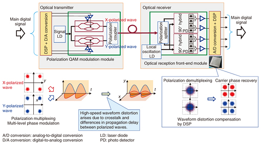
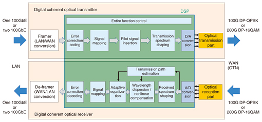
To avoid this problem, digital coherent optical transmission has been developed and adopted in 100-Gbit/s optical transport systems. This achieves highly efficient and stable long-distance transmission by not relying only on optical intensity but also using digital signal processing to utilize the phase and polarization of light, which are both properties of a light wave. The main modulation scheme applied to 100-Gbit/s optical transport is dual-polarization quadrature phase-shift keying (DP-QPSK). This modulates optical signals with four different phases and also uses the X-polarized wave and the Y-polarized wave to carry different signals. It achieves high receiving sensitivity by using coherent detection, in which a local oscillator light generates an interference signal with the received optical signal. From this interference signal, the intensity and phase information of the received optical signal is detected. The two polarization-multiplexed signals can be demultiplexed using digital signal processing. DP-QPSK achieves frequency utilization four times as high as that of OOK. Digital signal processing can also be used at the receiver to compensate for waveform distortions due to chromatic dispersion, polarization mode dispersion (PMD), and crosstalk between polarization signals on the optical fiber. Consequently, optical fiber transmission over more than 1000 km becomes possible without using optical compensation media such as dispersion compensating optical fiber. If the capacity of beyond 100G optical transmission systems is to be further increased, it is necessary to use higher multi-level modulation of optical signals such as dual-polarization 16-level quadrature amplitude modulation (DP-16QAM), which uses both optical intensity and phase. Different types of modulation can be generated by changing modulation signals generated using digital-to-analog (D/A) conversion in the same hardware of the transmitter/receiver including the optical modulator, driver amplifier, and optical receiver. This makes it possible to select the optimal modulation scheme depending on the channel capacity or transmission distance required. 3. DSP for beyond 100G optical transmissionWe have developed a real-time DSP for digital coherent optical transmission through an open innovation in which a number of organizations have participated [3, 4]. This work was supported by a research and development (R&D) project of the Ministry of Internal Affairs and Communications (MIC) of Japan and another project of the National Institute of Information and Communications Technology (NICT). In digital coherent optical transmission, the DSP performs modulation/demodulation and waveform distortion compensation. The functional configuration of the digital coherent optical transmitter/receiver used is shown in Fig. 3. We describe here an example of transmitting/receiving a 200-Gbit/s optical signal. In the transmitter, the framer converts the two 100-Gbit/s Ethernet (100GbE) signals input from the local area network (LAN) into two optical transport network (OTN) frame formats (optical-channel transport unit (OTU)4 signals) for the wide area network (WAN) and outputs them to the DSP. The DSP performs soft-decision error correction [5] with a redundancy of 20% or 25%, which provides strong error correction capability. The signals are then mapped onto four lanes (two orthogonal phases (phases I (in-phase) and Q (quadrature)) for each of the two orthogonal polarized waves (X- and Y-polarized waves)). After that, a pilot signal for estimating the status of the transmission path, for example, the OSNR, is added. Digital filtering for narrowing the optical signal spectrum is then applied. This is followed by D/A conversion. Finally, the optical transmission part converts the signals into 200-Gbit/s DP-16QAM signals and transmits them.
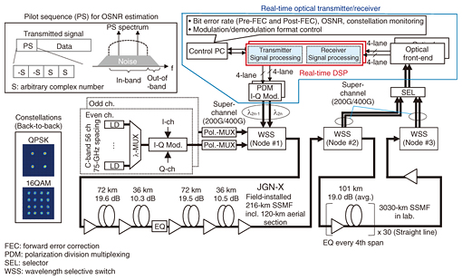
In the receiver, the optical receiver element mixes the received signal light with the local oscillation light to apply coherent detection and converts the light into four-lane analog signals as in the transmitter. The DSP converts the analog signals into digital signals and compensates for waveform distortion due to chromatic dispersion and optical nonlinear effects in the optical fibers [6, 7]. It then performs adaptive equalization, demodulation of the 16QAM signals, and error correction decoding. Thus, two OTU4 signals are obtained. The adaptive equalization element performs demultiplexing of the polarization-multiplexed signals and compensation for waveform distortion due to factors such as PMD. The transmission path estimation component rapidly estimates the in-band OSNR and the chromatic dispersion of the transmission path. With this information, it selects the optimal modulation method by using a pilot-aided bidirectional feedback channel between the transmitter and receiver [8] and performs rapid signal recovery [1, 2]. The entire function control element controls the coordinated operations of the different functional blocks within the DSP. The de-framer converts the two OTU4 signals into two 100GbE signals and outputs them to the LAN. If DP-QPSK is used for modulation, the transport rate becomes 100 Gbit/s, and only one 100GbE signal is handled. 4. 400-Gbit/s/ch real-time field transmission experimentA 400-Gbit/s/ch real-time adaptive modulation/demodulation experiment [9, 10] conducted using a real-time DSP and the Japan Gigabit Network-eXtreme (JGN-X) testbed is described below. The configuration of the field experiment system used is shown in Fig. 4. The system consisted of three photonic nodes (#1, 2, and 3). The nodes were interconnected by two types of fiber cable: a JGN-X field-installed testbed fiber cable (216-km single-mode fiber (SMF)) and a laboratory fiber (3030-km SMF). The JGN-X field-installed fiber was made up of fibers that were looped between the NICT Koganei headquarters and the TOKAI Chofu Repeater Station. The cable length was 18 km including a 10-km aerial section. Twelve fiber cores were used for the 216-km transmission line, with a 120-km aerial section. A gain equalizer (EQ) was inserted mid-span of the 216-km field fiber.
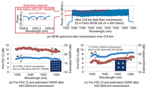
The transmission fiber in the laboratory consisted of 30 spans of 101-km standard SMF (SSMF) on a bobbin. Gain EQs were inserted at every fourth span (404 km). The even and odd channels of a continuous oscillation light from a laser diode (LD) light source that had been wavelength-division multiplexed with C-band 75-GHz spacing were modulated separately, and polarization-multiplexed signals were generated by a self-delayed polarization multiplexer (Pol.-MUX). They were then optically multiplexed by Node #1 to generate either DP-16QAM signals or DP-QPSK signals with 112 wavelengths (ranging from 1529.114 nm to 1562.283 nm) at C-band 37.5-GHz spacing as background WDM signals. Two real-time optical transmitters/receivers were prepared in order to generate super-channel signals, for example, 400-Gbit/s-2subcarrier (SC)-DP-16QAM and 200-Gbits/s-2SC-DP-QPSK signals. The real-time optical transmitter/receiver used Nyquist filtering to narrow the optical signal spectrum so that 400-Gbit/s or 200-Gbit/s super-channels with two wavelengths placed close to each other could be built. Node #1 replaced the two wavelengths (λ2n-1 and λ2n) of the background WDM signal with two different wavelengths from two real-time DSP-based transmitters. The real-time transmitter/receiver had a function for estimating the OSNR using a pilot signal [8]. This allowed adaptive modulation/demodulation. Namely, the OSNR of the received optical signal, which varied depending on the transmission distance, was estimated and used to select the appropriate modulation/demodulation scheme. In this experiment, adaptive modulation/demodulation transmission was carried out using an optical switch within Node #2 to change the transmission distance. Some results of an experiment with a 112-wavelength WDM signal having a total capacity of 22.4 Tbit/s are presented in Fig. 5. In this experiment, an OSNR of 20 dB was used as the threshold for determining whether DP-16QAM transmission was possible. After transmission over 216 km, the estimated OSNR was greater than the 20-dB threshold, indicating that DP-16QAM transmission was possible. The measured Q value before error correction of all the channels was about 6 dB, and we confirmed that the signals were free of errors after error correction. After transmission over 3246 km, the estimated OSNR was less than 20 dB. Therefore, DP-QPSK was selected instead. In this case, the Q value before error correction was also greater than 6 dB, and we also confirmed that the signals were error-free after error correction. This experiment verified that adaptive modulation/demodulation using an estimated OSNR is possible.
5. ConclusionThis article has described the latest trend in beyond 100G digital coherent optical transmission technology, which is the critical technology for building a high-capacity optical communication network that will provide a foundation for the coming full-fledged big data society. We will continue our R&D to enhance the performance and expand the application area of this technology. AcknowledgmentsThis work is partly supported by the R&D project on “Research and Development of Ultra-high-speed and Low-power-consumption Optical Network Technologies” of the MIC of Japan and the R&D project on “Research and Development of Optical Transparent Transmission Technology (Lambda Reach)” of NICT. We sincerely thank all concerned parties involved in the projects. References
|
||||||||||||||||||||||