|
|||||||||
|
|
|||||||||
|
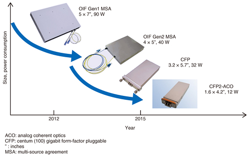
Feature Articles: Device Technology Development for Beyond 100G Optical Transport Network Vol. 14, No. 9, pp. 13–17, Sept. 2016. https://doi.org/10.53829/ntr201609fa3 Compact Optical Modulator and Coherent Optical Subassemblies for Beyond 100G Transport NetworkAbstractThis article presents an indium-phosphide-based optical modulator and a silicon-photonics-based coherent optical subassembly. Both devices enable compact and low-power beyond 100G (beyond 100 Gbit/s per wavelength) digital coherent transceivers that are essential for constructing an optical transport network economically. Keywords: coherent transceiver, InP, silicon photonics  1. IntroductionSteady progress has been made in the last few decades in expanding the transmission capacity of optical transport networks [1]. Recently, digital coherent technology with advanced modulation formats was proposed, which can significantly increase the transmission capacity of optical transport networks by incorporating ultrahigh-speed digital signal processing [2]. A commercial service employing 100-Gbit/s dual-polarization quadrature phase-shift keying (QPSK) systems is already in operation. Transceivers for the digital coherent technology need various components in order to support complicated modulation formats. However, there is strong demand for small-form factor pluggable digital coherent transceivers in order to expand their application space from long-haul networks to cost-sensitive metro areas and datacenter interconnections. The specifications of digital coherent transceivers such as power consumption and size are standardized at the Optical Internetworking Forum (OIF), where service providers, equipment vendors, and component vendors cooperatively develop implementation agreements (IAs) for optical networking products. The evolution of digital coherent transceivers, discussed at OIF, is shown in Fig. 1. The IA on the first-generation digital coherent transceivers, which were 5 × 7 inches (in) in size, was issued in 2011. Since then, the size and power consumption of these transceivers have been continuously reduced. At the second generation, the size was reduced to 4 × 5 in, and the latest IA at the OIF was for a centum (100) gigabit form-factor pluggable 2 - analogue coherent optics (CFP2-ACO) with a size of 1.6 × 4.2 in. Such compact transceivers facilitate high-density and low-power optical network equipment for metro networks and datacenter interconnects. Another aspect in regard to the evolution of the transceiver is the speed. If the transceiver can support beyond 100 Gbit/s per wavelength (beyond 100G) speed with the same form factor as 100 Gbit/s, the size required for a transmission capacity will be substantially reduced.
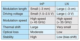
In this article, we present an indium-phosphide (InP)-based optical modulator and a silicon (Si)-photonics-based coherent optical subassembly (COSA). We first discuss the InP-based modulator, which was the key component to achieve the current generation CFP2-ACO transceiver. The InP-based modulator can achieve high speed with a compact size, and is promising for future very high-speed transceivers. Then, we discuss the Si-photonics-based COSA. The Si can integrate various kinds of optical devices on a single chip and will help to achieve an extremely compact transceiver. 2. InP-based optical modulatorNTT laboratories have developed a compact and high-speed InP optical modulator by making use of the superior optical properties of InP materials [3]. Table 1 summarizes the features of an InP and lithium niobate (LiNbO3: LN) modulator. Quantum confined stark effects in an InP-based multiple quantum well structure used in a waveguide core enable a large phase shift per unit length. Thus, the length of the phase modulation for an InP modulator can be reduced to as small as ~3 mm, which is one-tenth that for an LN modulator (~3 cm). In addition, the InP modulator can also provide low driving voltage (1.5–2.5 V). These features are beneficial for low-power operation.
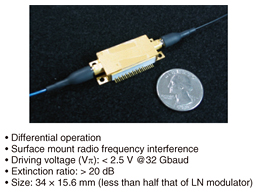
Furthermore, the InP modulator is free in principle from direct current bias fluctuation under operation, which is observed in LN modulators. A photograph and the features of our InP modulator are shown in Fig. 2. The modulator provides a driving voltage of less than 2.5 V while significantly reducing the footprint to half that of the LN modulator. The compact and low-power InP modulator technology makes it possible to achieve CFP2-ACO transceivers.
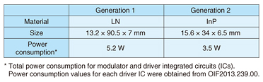
Table 2 compares the size and power consumption of the first- and second-generation optical modulators. A large portion of the power consumption in an optical modulator is determined by drivers. The power consumption of drivers for the LN and InP modulators is 5.2 W and 2.5 W, respectively. Even when taking into account the power consumption of a thermoelectric cooler (1 W) to maintain the operating temperature of the InP modulator, the total power consumption of the InP modulator (3.5 W) is still 1.7 W lower than that of the LN modulator.
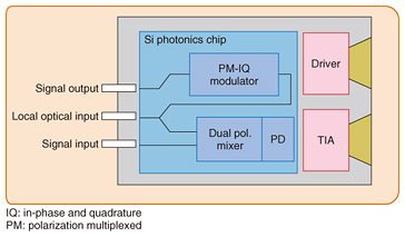
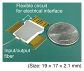
3. Si-photonics-based COSANTT laboratories have been developing a COSA based on Si photonics technology in order to further reduce the size of digital coherent transceivers. In digital coherent transport systems, the digital signal processor (DSP) not only demodulates signals but also compensates for signal distortion in the transmission line and analog devices. The powerful ability of DSP has opened up more choices in optical devices for the transceiver, including Si photonics, which uses microfabrication technology for LSIs (large-scale integrated circuits). Si substrates, which are transparent to 1.5-μm-wavelength light, are used as the platforms of photonic integration. NTT laboratories started research and development on Si photonic devices in 2000, foreseeing the potential of Si photonics [4]. Now, in addition to simple passive devices, high-speed optical modulators and germanium (Ge) photo detectors (PDs) can be integrated in Si substrates. The digital coherent transceiver has an optical modulator and drivers at the transmitter part and an integrated coherent receiver (ICR) at the receiver part. The ICR consists of 90° optical hybrids, high-speed PD arrays, a dual polarization mixer, and transimpedance amplifiers (TIAs) that convert the output current of PDs into a voltage signal. To date, these optical devices have been fabricated with different materials and connected with optical fibers. A function block for a COSA module is shown in Fig. 3. The key optical components are integrated in a single chip (Si photonics chip), and the drivers and TIAs are implemented in a package, as shown in Fig. 4. The subassembly eliminates the optical fibers and lenses that are conventionally used for connection between optical devices, resulting in an extremely small digital coherent transceiver.
4. ConclusionAn InP-based optical modulator and Si-photonics-based COSA are promising enablers for the future generation of digital coherent transceivers. The InP modulator is essential for future high-speed and long-distance transmission systems, and the COSA is essential for metro and datacenter interconnections. Both devices are key components for constructing cost-effective beyond 100G transport networks. NTT laboratories will continue to develop the key devices that contribute to the evolution of optical transmission networks. References
|
|||||||||