|
|||||
|
|
|||||
       |
Feature Articles: Photonics-electronics Convergence Devices that Support AI-IoT Service Era Vol. 15, No. 1, pp. 11–16, Jan. 2017. https://doi.org/10.53829/ntr201701fa2 Recent Progress in Optical Waveguide Technologies Enabling Integration of High-density Compact PhotonicsAbstractThe Internet of Things is expected to lead to the generation of various services in the near future and to bring changes to society. There will be a strong need for optical devices in order to achieve higher traffic capacity, greater economy, and compactness in future optical communication networks. This article reports the recent progress in the optical waveguide technologies being developed to meet these needs. Keywords: silica based, PLC, silicon nitride waveguide, plasmonics
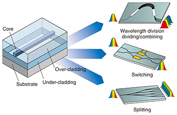
1. IntroductionIn addition to the recent spread of fiber-to-the-home services and the use of smartphones, the practical application of the Internet of Things (IoT) technology, in which everything is connected to the Internet, is expected to enrich society and provide a higher level of services. The optical network necessary to realize such a society requires circuits that enable various functions by processing light without converting it to electrons. These functions can be attained by using optical waveguides that pass light, as shown in Fig. 1. We can design various optical waveguides according to the required functions based on optical waveguide theory. These functions include switching the paths of light (optical switches), separating light into different colors, and bundling different colors into one (light filters). The waveguide functions are determined by the design, but the size of the waveguide and its optical properties are determined by the waveguide material.
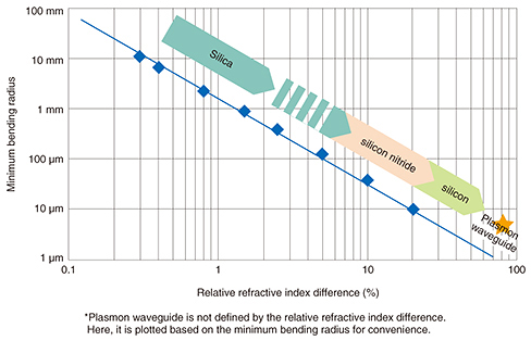
The relationship between the minimum bending radius and the relative refractive index difference of optical waveguides is plotted in Fig. 2. The relative refractive index difference is the ratio of the difference in the refractive index between the core into which the light is guided and the cladding that covers the core. As the relative refractive index difference increases, the minimum bending radius is reduced. This means that optical devices can be made more compact when we use materials that have higher refractive indices as waveguides. In the electronic device field, miniaturization and high integration of transistors have lowered the unit price of transistors in line with Moore’s law, while simultaneously increasing their performance. However, in the optical device field, the simple downsizing of optical devices using materials with a high relative refractive index difference may not always lead to improved performance because of their sensitivity to processing accuracy. There is generally a trade-off between the optical performance and the size of optical devices, and this trade-off prevents us from developing more highly integrated optical devices.
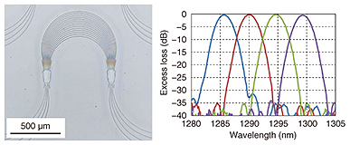
NTT laboratories are working to overcome this trade-off by trying to integrate appropriate materials and the refractive index difference into one optical device according to the application. In this article, we report on the recent progress made in optical waveguide technologies that is helping to achieve extremely compact and highly integrated optical devices. We describe four waveguide technologies in detail: high-performance silica-based planar lightwave circuit (PLC) technology, novel low loss silicon nitride (SiN) waveguide technology, plasmon waveguide technology that enables the fusion of electronic and optical devices, and three-dimensional optical via technology that enables the development of optical devices with the ultimate size. 2. Progress in silica-based PLCsSilica-based PLCs are optical circuits made of quartz glass, which is the same material as that used for optical fibers. Therefore, silica-based PLCs have excellent characteristics such as low-loss coupling with optical fibers and long-term reliability. Silica-based PLCs can precisely control light-propagation characteristics because of their low relative refractive index difference. Consequently, they are suitable waveguide platforms to achieve high-performance optical filters such those for as arrayed waveguide gratings (AWGs) that split and combine optical signals of different wavelengths. Several kinds of silica-based PLCs with these advantageous features have been widely introduced into optical communication networks. Commercially available silica-based PLCs have a minimum bend radius of about 1 mm (a relative refractive index difference of 1.5%) at present, and the size of general AWGs is 20–30 mm. We have increased the precision of waveguide fabrication and developed integration techniques that considerably reduce the chip size while maintaining the excellent properties of PLCs. A micrograph and transmission spectra of a precisely fabricated AWG with an increased relative refractive index difference of 5% are shown in Fig. 3. We achieved an AWG main optical circuit only 1 mm2 in size, as well as a low excess loss of only 0.2 dB with this AWG, which is comparable to commercially available AWGs.
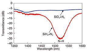
3. SiN waveguideSilicon (Si) nanowire waveguides, whose refractive index difference between the core and clad (delta) is ~40%, are useful for achieving ultra-small photonic-integrated circuits (PICs). However, there are several unresolved issues in fabricating high-performance optical devices using Si-nanowire waveguides. One of the key issues is in fabrication-error tolerance. For example, tolerable fabrication error is on the order of angstroms in order to meet the telecom-grade performance requirements of AWGs with Si-nanowire waveguides. This tolerance is not acceptable even if we use state-of-the-art fabrication technologies. SiN waveguides, whose delta (~20%) is between those of Si and silica, are promising candidates to maintain high fabrication tolerance with the relatively high integration. In particular, SiN waveguides formed by low-temperature plasma-enhanced chemical vapor deposition (PECVD) have attracted attention because they enable monolithic integration with modulators and detectors without causing thermal degradation. However, the conventional SiN waveguides formed by PECVD have large absorption loss in wavelengths around 1500 nm. This absorption is caused by the N-H bond, which is formed in the film by incorporating hydrogen dissociated from the silane (SiH4) gas source of the PECVD. To overcome the issue, we developed a hydrogen-free PECVD method by using a deuterated SiD4 gas source. The measured transmission spectrum of SiN waveguides (core size: 0.55 × 1.1 μm) formed by using the SiD4 gas source is shown in Fig. 4. The absorption peak at the wavelength around 1500 nm is much less than that of the conventional SiN waveguide formed by using SiH4 gas (red line). The propagation loss is 1.2 dB/cm, which is low enough to fabricate the PICs used in all telecommunications wavelengths. Note that Si, silica, and SiN waveguides can be monolithically integrated by forming spot-size converters using SiN waveguides. We are using this technology in attempts to fabricate high-performance PICs with various types of waveguides on Si photonics platforms.
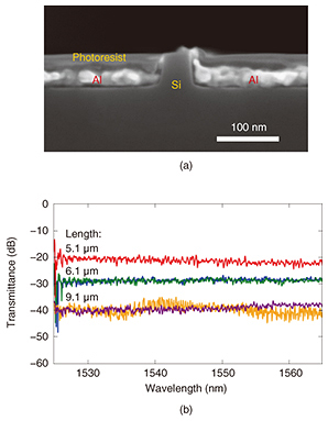
4. Plasmonic waveguideSi photonic devices have been attracting a great deal of attention as a promising technical basis for photonics-electronics convergence because their material varieties and fabrication processes are similar to those for Si electronic devices. In terms of device size, Si-nanowire waveguides have a much smaller cross section compared with legacy silica waveguides. Namely, the dimensions of Si-nanowire waveguides are typically several hundred nanometers, and they have 1/100 to 1/1000 the cross-sectional area of the legacy waveguides. However, the channel size of Si transistors has recently reached several tens of nanometers. Thus, there is still a one order of magnitude difference in the Si structure. We have developed plasmonic waveguide technologies [1] to further reduce the size of photonic devices. A plasmonic waveguide utilizes surface plasmon-polariton oscillation at metal-dielectric boundaries in order to obtain tight optical confinement within dimensions of several tens of nanometers. We can overcome the issue of the difference in size between photonics and electronics by using this waveguide as a base for optical devices. In addition, such tight optical confinement not only provides us with the advantage of a reduced device size but also several other advantages that improve optical-device performance. For example, some modulators utilizing the electro-optic effect have exhibited enhanced modulation efficiency as the electric-field intensity increases, which has led to reduced operational energy. A scanning-electron micrograph of a cross section of a fabricated plasmonic waveguide is shown in Fig. 5(a). It has an aluminum (Al)/Si/Al structure, and the Si core size is 60 × 60 nm. The transmittance spectra of fabricated plasmonic waveguides with various lengths are shown in Fig. 5(b). We confirmed an optical propagation loss of 4 dB/μm at 1550 nm, and we think the propagation loss can be reduced to less than 1 dB/μm by improving the fabrication process. Of course, this waveguide has higher loss compared with Si waveguides. In the future, we intend to explore the best-mix configuration with conventional dielectric photonic waveguides with the aim of achieving ultra-small, low-power-consumption optoelectronic systems for short-reach communications.
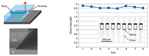
5. Optical through-hole-via technology using mirrorsThere are two ways of integrating high-density optical waveguide devices. One way is to reduce the bending radius of waveguides by using waveguides with a high relative refractive index difference. The other is to stack (pile up) the optical circuits. Moreover, when we stack the optical circuits, it also becomes easy to integrate optical circuits with different functions that involve the use of different materials. Of course, the circuits do not work as optical circuits if they are just stacked; it is necessary to couple them optically for each stacked layer. We call this configuration an optical through hole via (optical via), where the optical couplings function between different stacked optical layers. In particular, the path of propagating light in some layers is vertically changed toward other layers, and it is horizontally changed so that light propagates in the other layers when it reaches them with the optical via function. The technique of vertical light path conversion will become important when we can fabricate optical vias. We investigated how to achieve such light-path changes using mirrors at NTT Device Technology Laboratories. Mirror losses of fabricated eight-channel mirrors that indicate losses due to light-path changes are shown in Fig. 6. We confirmed low-loss light-path changes of less than 0.5 dB, which means the optical coupling loss between two layers was less than 1 dB. Therefore, our mirrors are promising for achieving low-loss optical via technology.
Reference
|
||||