|
|||||||||||||||||||||
|
|
|||||||||||||||||||||
       |
Feature Articles: Forefront of Research on Integrated Nanophotonics Vol. 16, No. 7, pp. 14–19, July 2018. https://doi.org/10.53829/ntr201807fa3 Toward Application of Plasmonic Waveguides to Optical DevicesAbstractThe size of a plasmonic waveguide is not limited by the optical wavelength. This enables plasmonic waveguides on the order of several tens of nanometers in length, which is not possible with dielectric waveguides, and exceptionally strong light confinement and efficient interaction with nanomaterials that have various unique properties become possible. However, such waveguides are not easily introduced in optical integrated circuits, so a three-dimensional plasmonic mode converter is required. Keywords: plasmonic waveguide, nanostructure fabrication, photonic integrated circuits
1. Enhancing interaction with plasmonic waveguides and related issuesThe use of nanomaterials*1 that have unique properties and functions has been increasing recently. The interaction between light and materials strongly affects device characteristics and is thus very important in implementing useful optical devices. However, the size scale of nanomaterials is small compared to optical wavelengths, so efficient interaction between light and nanomaterials is not easily achieved. To address this issue, NTT has been studying coupling systems for nanomaterials and photonic crystal nanostructures that are capable of strong light confinement, and we are developing the nanowire laser described in the article, “Compound Semiconductor Nanowire Laser Integrated in Silicon Photonic Crystal” [1]. However, optical elements that are conventionally used in optical integrated circuits, including photonic crystals, are generally based on dielectric materials. For that reason, the limit on the area of light confinement is determined by the optical wavelength. NTT is taking a different approach to address this issue by investigating optical device applications of plasmonic waveguides, which are not limited in size by the optical wavelength. Plasmonic waveguides can be extremely small, on the order of tens of nanometers. Our objective is to use these features to enhance the interaction of light and nanomaterials and realize the development of unprecedented optical devices. Plasmonic waveguides consist of metal and dielectric materials (semiconductors or insulators). Light propagates at the interface of the two materials as surface plasmons that accompany an electromagnetic wave. The electromagnetic wave is localized near the interface as near-field light, making it possible to confine the light in a region that is smaller than the light wavelength. Plasmonic waveguides can have various structures as combinations of metal and dielectric materials, but NTT has adopted the metal-insulator-metal (MIM) structure for research. In an MIM waveguide, light is concentrated in the insulator that serves as the core, so smaller cores produce stronger light confinement and a waveguide that has a small propagating mode. The core size of an MIM waveguide can thus extend into the deep-subwavelength regime*2, which is not possible with dielectric waveguides. That enables efficient interaction between light and nanomaterials, which holds promise for achieving optical devices that have unprecedented characteristics. However, deep-subwavelength MIM waveguides are not easily incorporated into optical integrated circuits. All plasmonic waveguides, including MIM waveguides, normally have associated absorption loss due to the metal. That loss becomes prominent when the core is small, and the loss can rise to about 1 dB/μm for cores in the deep-subwavelength regime, making it difficult to construct an optical integrated circuit with MIM waveguides alone. We therefore consider that the ideal configuration is to use MIM waveguides only for functional devices such as the optical detectors and modulators, while using conventional dielectric waveguides such as Si (silicon) waveguides for long-distance signal propagation. Implementing such a configuration requires highly efficient coupling of dielectric waveguides and deep-subwavelength MIM waveguides. However, the shape and size of the propagating modes of the deep-subwavelength MIM waveguide and the dielectric waveguide differ greatly, so a highly efficient plasmonic mode converter is needed.
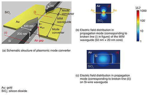
2. Design of plasmonic mode converterNTT has been working on a highly efficient plasmonic mode converter for conversion between a deep-subwavelength MIM waveguide that uses gold for the metal and air as the insulator, and a Si-wire waveguide (Fig. 1(a)) [2]. The propagating modes for the two types of waveguides differ greatly in size and shape (Fig. 1(b), (c)), so the mode conversion must involve a size reduction in both the lateral and vertical directions, which means that three-dimensional (3D) mode conversion is necessary. Lateral mode conversion between an MIM waveguide and a Si-wire waveguide has been reported previously [3–5], but those methods involved conversion between waveguides of about the same height and performed only two-dimensional (2D) mode conversion by compression only in the lateral direction with a laterally tapered structure. The use of a structure that is tapered in both the vertical and lateral directions has also been proposed as a means of 3D mode conversion [6], but the complexity of the fabrication process makes that approach impractical for application to optical integrated circuits.
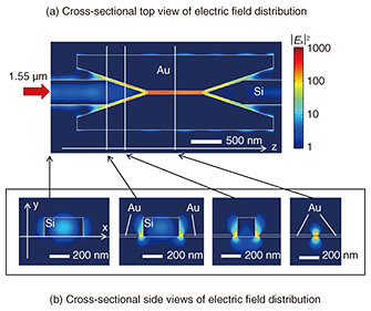
NTT therefore investigated a structure that can achieve highly efficient mode conversion for waveguides of greatly different heights with only a 2D tapered structure. We discovered that efficient mode conversion between a deep-subwavelength MIM waveguide and a Si-wire waveguide can be achieved by introducing a small air gap between the Si and the metal. The calculated propagating mode of 1.55-μm input light in a Si-wire waveguide, mode converter, and MIM waveguide is shown in Fig. 2. We can see from the figure that the side lobes of the propagating mode of the Si-wire waveguide are attracted to the metal parts placed near the Si waveguide, and there is coupling with the MIM waveguide that differs greatly in height via the air gap. The coupling efficiency depends on structure parameters such as the taper length ltaper and the air gap width wgap (Fig. 1(a)).
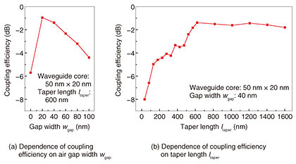
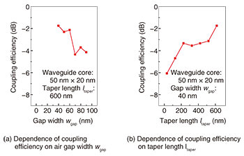
The coupling efficiency for various values of the air gap width is shown in Fig. 3(a). We can see from the figure that good coupling efficiency is not obtained without the air gap, but introducing a small air gap of about 20 nm dramatically improves the coupling efficiency. However, the coupling efficiency gradually decreases as the air gap width increases, and for a width of 100 nm, the coupling efficiency is the same as without the air gap. Furthermore, without the air gap, most of the propagating light is absorbed or scattered by the metal part of the mode converter. When the gap is wide, on the other hand, the side lobes of the Si-wire waveguide cannot be sufficiently attracted by the metal, and most of the light is scattered. We can thus see that a very small air gap is important to achieve efficient mode conversion. The taper length is also an important parameter in determining the coupling efficiency. The coupling efficiency for various taper length values is shown in Fig. 3(b). As the taper length increases, the coupling efficiency increases to reach a maximum in the vicinity of 600 nm and then decreases for longer taper lengths. Although longer taper lengths generally reduce loss in mode conversion, absorption by the metal reduces the coupling efficiency in a plasmonic mode converter because of loss due to absorption by the metal. The result obtained here shows that highly efficient mode conversion (about –1 dB) between a deep-subwavelength MIM waveguide (50 nm × 20 nm core) and a Si-wire waveguide (400 nm × 200 nm core) is possible with a mode converter that has a taper length of 600 nm and an air gap width of 20 nm. These predicted characteristics are very good in terms of coupling efficiency, converter length, and the reduction in waveguide core size compared to previously reported plasmonic converters of the same type.
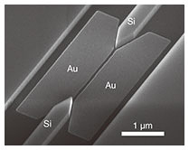
3. Fabrication and evaluation of plasmonic mode converterThe fabricated device comprises a Si-wire waveguide, a plasmonic mode converter, and an MIM waveguide. The Si-wire waveguide and the Si part of the plasmonic mode converter are fabricated on a silicon-on-insulator (SOI) substrate*3 by electron beam lithography and etching, and then the metal parts are formed by electron beam lithography and evaporation. This series of processes uses conventional nanostructure fabrication techniques and is therefore compatible with the processes used for other Si photonic devices. This enables integration with other optical devices on the same substrate, which is very important for device integration. A scanning electron microscopy image of the fabricated sample shows that the mode converter was fabricated with precise positioning (Fig. 4). We have successfully fabricated a plasmonic mode converter with an air gap width of 40 nm for an MIM waveguide that has a core size of 50 nm × 20 nm. Although the process described here may seem simple, it is not easy because of the positional accuracy required for fabrication at a scale of 20 nm or less. This process is possible with NTT’s high-level nanostructure fabrication techniques.
The coupling efficiency of a fabricated mode converter for an MIM waveguide that has a core size of 50 nm × 20 nm is shown in Fig. 5. The coupling efficiency in the fabricated mode converter is as high as –1.7 dB when the air gap width is 40 nm and the taper length is 600 nm, showing good agreement with the calculated value (–1.4 dB). The dependence of coupling efficiency on air gap with and taper length predicted from the calculation results is also exhibited for various air gap width and taper length values. We have achieved highly efficient mode conversion (–1.7 dB) between a deep-subwavelength MIM waveguide (50 nm × 20 nm core) and a Si-wire waveguide (400 nm × 200 nm core) with a mode converter that has a taper length of 600 nm and an air gap width of 40 nm. Furthermore, the core size of the connected MIM waveguide is (λ/n)2/2000 (λ: wavelength; n: refractive index). Previously, the smallest core size of the connected lateral MIM waveguide was (λ/n)2/120 [3], so these results indicate that we achieved a large reduction in the waveguide core size. Achieving highly efficient mode conversion with a taper length of less than 1 µm is also important for reducing the device footprint.
4. Future developmentWe have described here NTT’s efforts to introduce the size advantage of plasmonic waveguides to optical integrated circuits and also touched on the merits and problems of plasmonic waveguides. Development of the first highly efficient 3D mode converter enables introduction of waveguides that have a deep-subwavelength core to optical integrated circuits. In addition to reducing the size of conventional devices, this achievement paves the way for the potential implementation of unprecedented new devices in combination with nanomaterials that have unique properties. References
|
||||||||||||||||||||