|
|||||||||
|
|
|||||||||
|
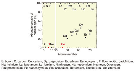
Feature Articles: Creating Novel Functional Materials Vol. 17, No. 10, pp. 12–17, Oct. 2019. https://doi.org/10.53829/ntr201910fa3 Magnetically Purified Erbium-doped Oxide Crystal—Towards Creating a Quantum-information-manipulation PlatformAbstractErbium (Er) is a rare-earth element that is expected to be a platform for manipulation of quantum information by utilizing telecommunication-wavelength photons. However, high-quality epitaxial growth of Er-doped host crystals is difficult, and the memory time of quantum information, which determines the performance of quantum manipulation, is much shorter than theoretically predicted. We investigated a good-compatibility rare-earth oxide as a host crystal for Er. The host oxide crystal, cerium oxide (CeO2), had its nuclear spin removed (i.e., magnetically purified). The nuclear spin is the main factor that shortens the lifetime of quantum-information retention time. In this article, we describe high-quality epitaxial growth of CeO2 and its optical properties as a thin film grown on a silicon substrate. Keywords: rare-earth oxide, erbium, molecular beam epitaxy  1. Erbium-doped oxide and its application as a quantum-state-manipulation platformIt has long been known that adding rare-earth atoms to uniform solid crystals forms a determinative, discrete, and less-fluctuating ideal energy quantum level that is robust against changes in the external environment such as differences in host materials and temperature. This is because rare-earth atoms have a unique electron configuration; that is, their 4f electron orbit is electrically shielded from the outside world. In recent years, researchers have been actively studying the application of such superior quantum levels of rare-earth atoms as the platforms of quantum-information-manipulation devices (especially photon memories) used in quantum-information communication. Quantum-information manipulation is defined as follows: photons responsible for the transmission of quantum information are transferred to electrons in a material, some operations are added to the electron state, and the photons are re-emitted as photons carrying that information. At that time, the electronic state (quantum level) of the material to which the information is transferred must have a slight fluctuation in energy (so that a long time is taken to lose any quantum information). A rare-earth atom is outstanding as an element that meets this requirement. Of the rare-earth elements, only erbium (Er) can interact with the optical-telecommunication photons (i.e., those having a wavelength of 1.55 µm). Accordingly, Er-doped crystals are promising as a platform for quantum-information-manipulation devices in quantum optical communication using existing optical-fiber networks [1]. The question that arises is what kind of Er-doped crystals are specifically required. First, Er needs to be added in a diluted manner. That is because if the distance between the doped Er atoms is too close, energy (i.e., quantum information) will be exchanged between the Er atoms, and the information will be lost instantaneously [2]. The distance between Er atoms must therefore be sufficient so that the atoms are separated (diluted). Moreover, the host crystal to which Er is added strongly influences the quantum level characteristics of Er, particularly the degree of fluctuation of quantum levels. For example, when each atom that composes the host crystal has nuclear spin, large magnetic fluctuation occurs, and the quantum level fluctuation becomes large. This fluctuation is also a factor contributing to losing quantum information in a short time. For more efficient manipulation of quantum information, it is necessary to strongly confine the light in the host crystal and enhance its interaction with Er. Technology for fabricating optical circuits (e.g., optical resonators, waveguides, and multiplexing/demultiplexing devices) used in silicon (Si) photonics is useful to achieve this. It is therefore desirable to form the host crystal as a thin film on a Si substrate. Some rare-earth oxides are candidate materials that can be grown as thin films on a Si substrate with less magnetic fluctuation. The crystal structure of a rare-earth oxide is similar to that of Si, and its lattice constant is exactly twice that of Si. This indicates that epitaxial growth of such an oxide on a Si substrate is possible. Among the many rare-earth atoms, only cerium (Ce) has no nuclear spin (Fig. 1). Thus, Ce has excellent characteristics; namely, it has no magnetic fluctuation and does not affect the quantum state of Er.
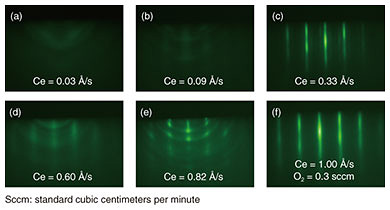
Incidentally, since the natural abundance ratio of isotopes with nuclear spin is very small for oxygen, cerium oxide (CeO2) is the most promising candidate for an Er-doped host crystal on a Si substrate. However, although CeO2 has been studied as a polishing agent, reduction catalyst, and other purposes [3], there are no published research examples of it being used as an Er-doped host crystal—as the basis of a quantum-information manipulation platform—or as an epitaxial-crystal thin film on a Si substrate. 2. Crystal growth of Er-doped CeO2 thin filmsAn Er-doped CeO2 film was grown to a thickness of 30 nm at 640°C on a surface-cleaned Si (111) substrate by using molecular beam epitaxy [4]. The rare-earth materials used, high-purity (> 99.99%) Er and Ce metals, were oxidized with O* (oxygen-atom radicals) to form a rare-earth oxide film. To obtain high-quality crystals of CeO2 as a host matrix, it is necessary to adjust the supply ratio of Ce and O* so that the formed thin film has a stoichiometric composition (in this case, a stoichiometry of Ce:O = 1:2). Crystal quality was therefore investigated by changing the amount of Ce supply under a constant O* supply. Reflection high-energy electron diffraction (RHEED) images after crystal growth are shown in Fig. 2. When the amount of Ce supplied is small and the oxidizing power is excessive (Fig. 2(a), (b)), the halo-like pattern (showing an amorphous state) is obtained, and when the amount of Ce supplied is large and the oxidizing power is insufficient (Fig. 2(d), (e)), ring-like patterns (showing a polycrystalline state) appear.
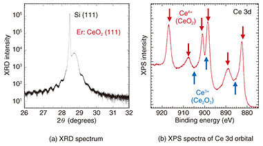
In contrast, in Fig. 2(c), a streak pattern (indicating a flat surface and single-crystal growth) is observed, and it can be seen that a thin film close to stoichiometry is formed by supplying that amount of Ce. It can also be seen that the streak pattern is maintained even when each supply amount is increased while the supply ratio of Ce to O* is kept constant (Fig. 2(f)). Therefore, when Er is added as a dopant, it is possible to change the Er concentration while keeping the crystal quality constant by changing the crystal growth rate of the host CeO2 crystal. In addition to the cubic fluorite structure targeted in this study, CeO2 has multiple crystal structures such as cubic bixbyite (Ce2O3) and hexagonal. Since the above-described RHEED images cannot distinguish these differences in crystal structure, the crystal structure was examined in more detail by using X-ray diffraction (XRD) spectroscopy and X-ray photoelectron spectroscopy (XPS). The crystal lattice spacing estimated from the XRD spectrum shown in Fig. 3(a) is 3.11 Å, which corresponds to cubic CeO2 and indicates that the hexagonal crystal structure does not exist. Moreover, from the spacing of the periodic satellite peaks observed when the crystal is grown uniformly at the atomic level, it is clear that the thickness of the grown CeO2 film is 26.4 nm, which agrees fairly well with the assumed grown-film thickness. The charge states of the Ce atoms, estimated from the XPS spectra of the Ce 3d orbital shown in Fig. 3(b), are all Ce4+ in the case of fluorite CeO2, and Ce3+ does not exist in the case of bixbyite Ce2O3. The above results demonstrate that the grown CeO2 thin film is the desired cubic fluorite CeO2.
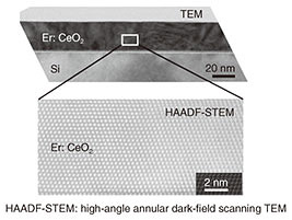
A cross-sectional TEM (transmission electron microscopy) image of the grown Er-doped CeO2 is shown in Fig. 4. From this image, it can be seen that in addition to an extremely flat surface, a very high quality Er-doped CeO2 thin-film crystal without crystal defects or different crystal-structure phases is obtained. It is thus concluded that a high-quality Er-doped CeO2 thin film was epitaxially grown on a Si substrate for the first time.
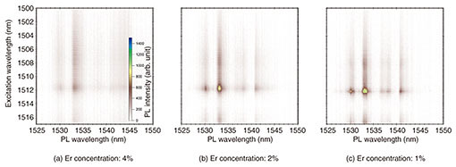
3. Optical properties of Er-doped CeO2 thin-film crystalThe optical properties of the high-quality Er-doped CeO2 thin-film crystals were investigated. Color plots of the dependence of photoluminescence (PL) on excitation wavelength are shown in Fig. 5. In the PL measurement, energy is applied to a sample by irradiating the sample with a laser to excite electrons in the sample to a high-energy (excitation) state, and the light emitted when these excited electrons return to a low-energy state is observed. In this investigation, the Er concentration was changed from 4% (Fig. 5(a)) to 1% (Fig. 5(c)), and the PL measurement was performed at a temperature of 4K. It can be seen that for all Er-doping concentrations, sharp PL emission appears at a PL wavelength (horizontal axis) of 1533 nm against an excitation wavelength (vertical axis) of 1512 nm. This result indicates that the dopant Er atoms replace Ce sites in the parent CeO2 crystal and are optically activated. In other words, in this Er-concentration range, Er atoms do not exist between crystal lattices, or they form Er clusters. Multiple PL emission peaks appear because the energy level of the doped Er is split due to the crystal field of the CeO2 host.
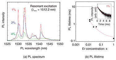
This emission spectrum is compared in detail in Fig. 6(a). For all Er concentrations, the emission peak appears at the same wavelength; at the same time, the emission intensity increases as Er concentration decreases. This result can be explained by the fact that as Er concentration decreases, the distance between the Er atoms increases, so the Er atoms become isolated in the host crystal. As a result, the non-emission process involving energy transfer by Er-Er atomic interaction is suppressed (and emission efficiency is enhanced). This suppression of the non-radiative process by diluting the doped Er also changes the PL-emission lifetime. The dependence of PL-emission lifetime on Er concentration is shown in Fig. 6(b). The PL-emission lifetime is measured by the intensity change of the emission from the sample appearing after the laser irradiation in the time domain (inset of Fig. 6(b)). It is clear from the figure that the PL-emission lifetime is extended as the Er concentration is reduced. The dotted line in the figure shows a PL-emission lifetime of about 11 ms when 0.001% of extremely dilute Er is added to a YSi2O5 host crystal (which has conventionally been used as a quantum optics crystal), and that value is considered to be the intrinsic PL-emission lifetime of Er in a solid; that is, the Er-Er atomic interaction can be ignored.
For the Er-doped CeO2 used in this investigation, the minimum Er concentration was 1%. By lowering the Er concentration by another order of magnitude, it is expected that (i) the Er-Er interaction can be completely suppressed, and (ii) the Er atoms can be completely isolated in the solid. Also, in regard to the PL-emission characteristics, we observed the formation of a definite energy state, enhancement of PL-emission efficiency, and prolongation of PL-emission lifetime. In conclusion, Er-doped CeO2 thin films with high quality in terms of both crystal structure and optical characteristics were successfully obtained. 4. Future developmentIt is expected that with the high-quality Er-doped CeO2 thin film obtained in this investigation, the memory time of quantum information will be longer than that possible with a conventionally doped host crystal. We plan to fabricate an optical waveguide structure on a crystal surface in order to evaluate the quantum-information memory time and achieve on-chip manipulation of the quantum state by using telecom-band photons. References
|
|||||||||