|
|||||||||||||
|
|
|||||||||||||
|
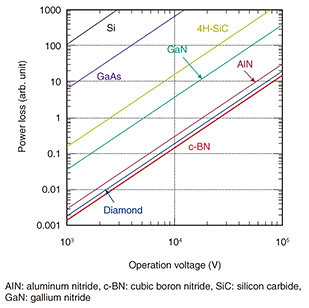
Feature Articles: Creating Novel Functional Materials Vol. 17, No. 10, pp. 30–35, Oct. 2019. https://doi.org/10.53829/ntr201910fa6 Development of Next-generation Wide-bandgap SemiconductorsAbstractCubic boron nitride (c-BN) is a wide-bandgap semiconductor with the highest breakdown field among semiconductors. It has the potential to dramatically improve efficiency in power devices. Although c-BN is a metastable material, we have heteroepitaxially grown high-quality c-BN thin films by developing a unique growth technique. We have also used doping to control the electrical conductivity of the c-BN films. These accomplishments are major steps toward the fabrication of c-BN-based power devices. Keywords: cubic boron nitride (c-BN), diamond, next-generation wide-bandgap semiconductors  1. Power device applications of wide-bandgap semiconductorsWide-bandgap semiconductors are expected to serve as components of high-efficiency power devices, in which electrical power loss is significantly lower than in conventional semiconductor-based power devices. Here, silicon (Si) and gallium arsenide (GaAs) are typical conventional semiconductors. The main functions of power devices include regulation of direct current (DC) voltage, frequency conversion of alternating current (AC) voltage, and conversion between AC and DC. For example, in AC adapters used in personal computers and mobile phones, power devices convert the voltage from AC 100–200 V to DC ~20 V. The relationship between power loss and operation voltage of power devices consisting of various semiconducting materials is shown in Fig. 1. Power loss is determined by the on-resistance of power devices; it becomes smaller with lower on-resistance. Increasing the carrier concentration and reducing the current-path length are both effective in reducing the on-resistance, and consequently the power loss.
Such conditions are more readily fulfilled when the breakdown field*1 of the constituent semiconductor is higher. The high breakdown fields of wide-bandgap semiconductors, at least one order of magnitude higher than those in Si or GaAs, means that the on-resistance of the power devices can be reduced by three orders of magnitude. As a result, wide-bandgap semiconductor-based power devices can operate more efficiently with lower power losses. Some wide-bandgap semiconductor-based power devices are already in practical use, as exemplified by silicon carbide (SiC)- or gallium nitride (GaN)-based ones, including high-efficiency inverters for trains. At NTT Basic Research Laboratories, we have been studying next-generation wide-bandgap semiconductors such as cubic boron nitride (c-BN), aluminum nitride (AlN), and diamond. In the following sections, we describe the growth of c-BN thin films with the highest breakdown field among semiconductors and describe how we control their electrical conductivity. The power loss in c-BN-based power devices is expected to be four orders of magnitude lower than those in Si- or GaAs-based ones and at least one order of magnitude lower than those in SiC- or GaN-based ones (Fig. 1). If such high-efficiency c-BN-based power devices become available, power loss can be significantly reduced in electrical vehicles, railways, and solar-power and wind-power generation systems. Accordingly, research aimed at developing c-BN-based power devices is underway, as this approach uses fewer natural resources and will contribute to constructing a sustainable society on a global scale.
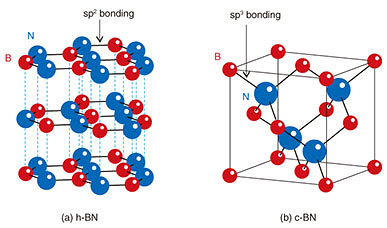
2. Growth of c-BN epitaxial films using unique growth techniqueBoron nitride (BN) is a compound semiconductor composed of boron and nitrogen. BN can have several crystal structures depending on the bonding character and stacking sequence. Representative crystal structures of BN are shown in Fig. 2. The thermodynamically stable phase under standard temperature and pressure is sp2-bonded hexagonal BN (h-BN). In contrast, sp3-bonded c-BN is a high-pressure and high-temperature stable phase, that is, a metastable phase under standard temperature and pressure.
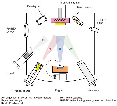
To utilize c-BN with a high breakdown field for power devices, first of all, the growth of phase-pure (i.e., composed of only the sp3-bonded phase) c-BN films is necessary. Ion irradiation to the growth surface is known to be effective for forming the metastable sp3-bonded c-BN phase. Nevertheless, growth of a phase-pure c-BN thin film has been hampered by partial formation of the thermodynamically stable sp2-bonded BN phase. The sp2-bonded BN phase has a disordered h-BN structure and is called turbostratic BN (t-BN). The inclusion of the t-BN phase prevents epitaxial growth and renders the resultant BN films polycrystalline ones. Despite the above-mentioned difficulties, we have grown phase-pure c-BN films by developing a unique growth technique, that is, ion-beam-assisted molecular beam epitaxy (MBE) (Fig. 3). Boron (B) atoms are supplied from an electron beam evaporator, while nitrogen radicals (N*) are supplied from an RF (radio frequency) radical generator. At the same time, the growth surface is irradiated with argon ions (Ar+). The Ar+/B ratio was found to play a crucial role in forming the sp3-bonded BN [1, 2]. The substrate is diamond with a small lattice mismatch with c-BN.
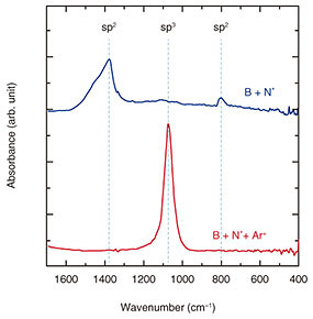
To investigate the effect of the Ar+ irradiation during the BN growth on the bonding characteristics and crystal structures of the resultant BN films, we first grew BN films without and with Ar+ irradiation. The Fourier transform infrared spectroscopy (FT-IR) absorption measurement*2 of the samples prepared without and with Ar+ irradiation is shown in Fig. 4. In the absence of Ar+ irradiation, two absorption peaks were observed at around 800 cm–1 and 1380 cm–1, which are attributed to sp2-bonded BN. No absorption peak related to sp3-bonded BN was observed. This means that the sp2-bonded BN film was grown.
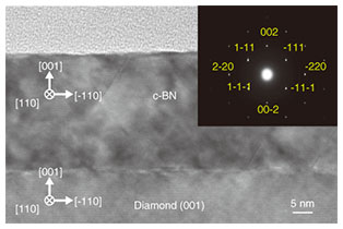
In contrast, in the presence of Ar+ irradiation, only an absorption peak was observed at around 1070 cm-1, which is attributed to the sp3-bonded BN. No other peaks originating from sp2-bonded BN were observed. Therefore, the grown film is phase-pure sp3-bonded BN. Accordingly, the ion irradiation allows for a selective formation of the sp3-bonded BN. We surmise that the kinetic energy and/or momentum transferred from the Ar+ ions to the growth surface may contribute to the preferential formation of the sp3-bonds in BN. To identify the crystal structure, we performed cross-sectional TEM (transmission electron microscopy) measurement for the BN film prepared with the Ar+ irradiation, which was phase-pure (sp3-bonded BN) judging from the FT-IR measurement (Fig. 5). The BN film is grown uniformly from the heterointerface (interface between the diamond substrate and the BN film) to the surface. The inset in Fig. 5 shows a selective-area electron diffraction pattern of the BN film. All the diffraction spots are assigned to those for single-crystal c-BN (001) taken along the [110] zone axis. No other spots or ring patterns attributed to sp2-bonded BN are observed. Therefore, we can conclude that the single-crystal c-BN (001) film is heteroepitaxially grown on the diamond (001) substrate [3].
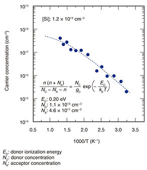
3. Electrical conductivity control in c-BN filmsTo fabricate power devices, it is necessary to grow n-type and p-type c-BN films and control their electrical conductivity. For c-BN, Si and S (sulfur) serve as donors, while Be (beryllium) serves as an acceptor. We carried out the n-type doping first; Si was supplied as a dopant during the epitaxial growth of the c-BN (001) films by using a K-cell (Knudsen cell).*3 The dependence of carrier concentration on temperature for a Si-doped c-BN film with a Si concentration ([Si]) of 1.2 × 1018 cm–3 is shown in Fig. 6. The carrier concentration monotonically increases with the measurement temperature. The carrier concentrations at room temperature (RT) and 500°C are respectively 2.1 × 1015 cm–3 and 6.0 × 1017 cm–3. From the fitting with the equation for the charge neutrality condition (Fig. 6, inset), the donor ionization energy (ED), donor concentration (ND), and acceptor concentration (NA) are respectively estimated to be 0.20 eV, 1.1 × 1018 cm–3, and 4.6 × 1017 cm–3. Because ND is almost the same as [Si], most of the doped Si atoms are considered to be substitutionally incorporated into boron sites, where they then serve as donors. Remarkably, ED of 0.20 eV is lower than those for other next-generation wide-bandgap semiconductors such as AlN and diamond. The low ED in c-BN is promising for higher carrier concentration and lower resistivity, suggesting the potential of c-BN to exceed AlN or diamond, once a c-BN-based power device is achieved.
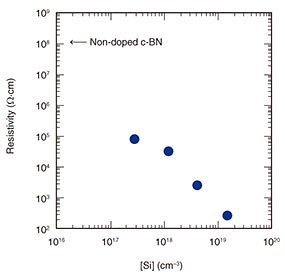
The dependence of the resistivity on [Si] at RT for the Si-doped c-BN films is shown in Fig. 7. For comparison, the resistivity of the non-doped c-BN film is also plotted in Fig. 7. The resistivity of the non-doped c-BN film is as high as ~108 Ω·cm, while the Si-doped c-BN film with a [Si] of 1.5 × 1019 cm–3 shows low resistivity of ~260 Ω·cm. The resistivity decreases as [Si] increases, demonstrating the successful control of electrical conductivity by varying the dopant concentration, in this case, [Si].
4. SummaryWe described the recent progress in research on c-BN at NTT Basic Research Laboratories. We have achieved the epitaxial growth of single-crystal c-BN thin films and control of electrical conductivity in n-type Si-doped c-BN films. These accomplishments are important steps toward the fabrication of electron devices. Further improving crystalline quality and p-type doping will pave the way to achieving high-performance c-BN-based power devices. References
|
|||||||||||||