|
|||||||||||||||||
|
|
|||||||||||||||||
|
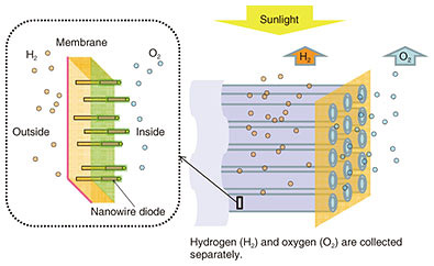
Feature Articles: Creating Novel Functional Materials Vol. 17, No. 10, pp. 36–41, Oct. 2019. https://doi.org/10.53829/ntr201910fa7 Crystal Growth of Wurtzite GaP Nanowires for Solar-water-splitting DevicesAbstractGallium phosphide (GaP) is an environmentally friendly III-V semiconductor, and it has an indirect bandgap as a stable zincblende structure. However, if controlled nanowire growth is carried out, a wurtzite structure with a direct bandgap can be achieved. We successfully grew wurtzite GaP nanowires without stacking faults by using our original method using chlorine etching and repeated gallium supply. We present here our results of solar-water splitting using a p-type nanowire photoelectrode, and we explain the fabrication and properties of a pin-type nanowire solar cell. Keywords: nanowire, gallium phosphide, solar-water splitting  1. Nanowire solar-water-splitting deviceResearch and development to harvest solar energy that is inexhaustible and clean has been progressing as part of efforts to achieve a sustainable society. In 1972, Fujishima et al. reported on water and carbon dioxide reduction using a semiconductor photoelectrochemical method for the first time [1]. Their method is promising for producing fuel and organic substances that can be stored and is still being researched actively. The redox (reduction oxidation reaction) process of water using sunlight (solar-water splitting) is the simplest process because the products are hydrogen and oxygen. For this reaction, the potential difference between cathodes and anodes in an electrochemical system must be larger than 1.23 V (thermodynamically required). In addition, the materials used for solar-water splitting should be selected in consideration of low toxicity, abundance on earth, and long stability without corrosion during the reaction. Photocatalysts composed of fine powders have also been studied for solar-water splitting, but their solar-to-hydrogen conversion efficiency is low at present (about 1–2%). In practical use, an ideal device is to produce hydrogen and oxygen separately. Our target device considering the above points is shown in Fig. 1 [2]. The transparent tube-like structure contains dense nanowire diodes with both ends exposed to water. When the nanowire diodes absorb sunlight, the generated electrons react with hydrogen ions at the cathode side of the nanowires (outside the tube) to form hydrogen, and the holes react with water at the anode side of the nanowires (inside the tube) to form oxygen. Keeping the hydrogen and oxygen separate makes their collection easier.
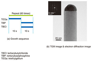
Here, individual nanowire diodes independently contribute to light absorption and water splitting. Even if some nanowires fail, the device performance of others should not be affected. Since nanowires are small in diameter, we can grow good heterostructures using various materials with a relatively large difference in the lattice constant. Therefore, some semiconductors with different bandgaps can be connected axially and absorb a wide wavelength range of sunlight. In principle, such a tube-like structure can be fabricated by embedding a myriad of nanowire diodes on the substrate surface with a transparent resin, exposing the nanowire tips, peeling the resin film off the substrate, and rounding it. There are many challenges to achieve this target device. The growth of nanowires requires a good structure with uniform length and thickness and high density. In addition, techniques to grow different materials in the axial direction and to control the concentration of dopants are also required. For photoelectrochemical devices, it is necessary to develop a proper coating film with optical transparency and corrosion protection as well as cocatalysts to promote chemical reactions at the nanowire ends. The road to achieving the target device is long, but we have made progress by growing wurtzite gallium phosphide (GaP) nanowires. We have also performed p- and n-type doping in nanowires and solar-water splitting using nanowire electrodes, and we have fabricated nanowire solar cells [3, 4]. These achievements are explained in this article. 2. Wurtzite GaP nanowiresTypical GaP materials are III-V semiconductors with an indirect bandgap and are not used for high-performance devices because of their poor electronic conduction and optical absorption characteristics. However, because GaP is composed of elements abundantly present on the earth, it is suitable as a material for solar cells and photoelectrodes, which must be inexpensive and have large areas. Since the bandgap is 2.1 eV, it is possible to perform solar-water splitting without bias if the voltage loss at the electrode is small. Band structure calculations predicted that wurtzite GaP has a direct bandgap, although stable GaP normally has a zincblende structure. A research group in Europe successfully carried out crystal growth of wurtzite GaP nanowires for the first time recently, and those nanowires showed a large increase in photoluminescence compared with zincblende GaP [5]. We also succeeded in carrying out crystal growth of wurtzite GaP nanowires [4]. The growth was carried out with the vapor-liquid-solid (VLS) method*1 using gold nanoparticles as catalysts. First, gold particles were dispersed on the substrate, and then the source gases were supplied at 400–500ºC in the crystal growth apparatus. As shown in Fig. 2(a), TBCl (tertiarybutylchloride) was used as a chlorine etching material, and TEGa (triethylgallium) as a group III source and TBP (tertiarybutylphosphine) as a group V source were supplied alternately. This technique enabled us to successfully grow wurtzite GaP nanowires without stacking faults. A transmission electron microscope (TEM) image and an electron diffraction pattern of one wurtzite GaP nanowire are shown in Fig. 2(b). The nanowires were about 500 nm in length, and the diameter of the gold particles was about 40 nm. The TEM image shows the gold part as hemispherical black material at the nanowire tip. The electron diffraction pattern indicates a typical wurtzite structure. The TEM image also shows that the nanowires have smooth sidewalls without stacking faults.
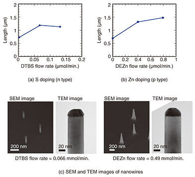
3. Impurity doping in nanowiresIn growing the GaP nanowires, we tried to incorporate zinc (Zn), a p-type dopant, and sulfur (S), an n-type dopant, into the nanowires. The p-type dopant source was diethylzinc (DEZn), and the n-type dopant source was DTBS (ditertiarybutylsulfide). Graphs of nanowire lengths versus flow rates are shown in Fig. 3(a, b), and scanning electron microscope (SEM) and TEM images of the nanowires are shown in Fig. 3(c). The lengths of the nanowires changed with the Zn and S doping. In particular, the length of the p-type ones obviously increased as the flow rate of DEZn increased, and they became wider at the bottom. These results show that the variation of the growth rate should be taken into account when fabricating devices by performing impurity doping. The TEM images show that both types of nanowires had some stacking faults due to doping, but they still had wurtzite structures.
Impurity and carrier concentrations were evaluated by secondary ion mass spectrometry (SIMS)*2 measurements and Mott-Schottky plots*3 from electrochemical experiments. The nanowire-grown samples were embedded in a resin or SiO2 (silicon dioxide) film by sputter deposition and measured as average concentrations. It was confirmed that the concentration of impurities and carriers in the nanowires increased as the flow rates of the dopant sources increased. A concentration of about 1018 cm–3 was obtained for both types of doped samples for both carrier and impurity. Since the measurement methods used here provide average information on a large number of dispersed nanowires, we will continue to consider a method for measuring individual nanowires for more accurate measurements.
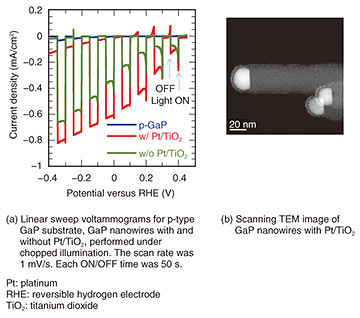
4. Solar-water splitting using nanowire electrodesWe grew p- and n-type wurtzite GaP nanowires and conducted photoelectrochemical experiments in order to achieve solar-water-splitting devices. The results obtained using a p-type sample as a photocathode electrode are shown in Fig. 4. In Fig. 4(a), we compare a p-type GaP substrate and p-type GaP nanowire samples.
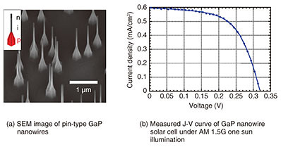
We also compared nanowires with and without platinum (Pt) nanoparticles (as cocatalyst) / titanium dioxide (TiO2) protective thin film. The TEM image of GaP nanowires with Pt/TiO2 is shown in Fig. 4(b), where the TiO2 thin film covers the nanowire uniformly and Pt fine nanoparticles are dispersed. In the photoelectrochemical experiments, photocurrent was measured by repeating ON/OFF of the light while scanning the voltage using simulated sunlight (Solar simulator, AM 1.5G). The electrolyte was a 0.5-M H2SO4 (sulfuric acid) aqueous solution, and the counter electrode was a Pt plate. Compared with the GaP substrate, the photocurrent output of the nanowire samples was found to be large. We also confirmed that the nanowire sample with TiO2 dispersed with Pt fine nanoparticles showed no degradation of nanowires. The density was evaluated to be 70–110 μm−2, which was relatively high, but the photocurrent itself was lower than expected due to the fact that the nanowires could not be made longer than 1 μm and the length of nanowires varied. Similar measurements were carried out on n-type nanowires. However, degradation due to corrosion was severe, even for samples with the TiO2 protective film. We therefore need to investigate the optimum protective film for n-type photoanode electrodes. 5. Nanowire solar cellSince the final target of the solar-water-splitting device includes pin-type nanowire photodiodes, we grew pin-type nanowires and examined the solar cell characteristics. An SEM image of the grown pin-type nanowires is shown in Fig. 5(a), and the photocurrent voltage plot measured using simulated sunlight after device fabrication is shown in Fig. 5(b). The device was fabricated by depositing 5 nm of alumina on the sample surface using atomic layer deposition, embedding the nanowires in resin for planarization, exposing the nanowire tips, and then forming electrodes on the back of the substrate and the sample surface. ITO (tin doped indium oxide) was used for the transparent electrode on the sample surface. The lengths of the p-, i-, and n-segments were designed to be 330, 1300, and 330 nm, respectively. The p-type segments were tapered by doping as described above, resulting in a structure with a large bottom diameter as shown in the schematic illustration. The measured result was fitted with a diode model of the following equation. J = Jsc – (V – Rs J) /Rp – J0 exp(q (V – Rs J)/(n k T) – 1), where q is the electron charge, k is the Boltzmann constant, T is the absolute temperature, Jsc is the short-circuit current density, Rs is the series resistance, Rp is the parallel resistance, J0 is the saturation current density, and n is the ideal factor. The voltage at J = 0 is the open-circuit voltage Voc.
The result was Jsc = 0.6 mA/cm2, Voc = 0.32 V, J0 = 4.63×10⁻⁸ A/cm2, n = 1.33, Rp = 6.5 kΩ·cm, and Rs = 40 Ω·cm, and the conversion efficiency of this sample was 0.11%. This low efficiency is due to the low nanowire density (9.8×107 cm–2). On a single nanowire basis, Jsc = 160 mA/cm2. This large photocurrent is due to the effect of the nanowires collecting the ambient light. Therefore, by optimally designing nanowire solar cells, we can expect to achieve highly efficient solar cells. 6. Future developmentThrough our experience in fabricating nanowire photoelectrodes and nanowire solar cells, we were able to get closer to our target solar-water-splitting devices using wurtzite GaP nanowires. The nanowires absorb light efficiently, and a large photocurrent can be expected, but a large open-circuit voltage of about 2 V, which is sufficient for water splitting, is considered to be difficult when using a single pin-type nanowire diode. Therefore, we are planning to form a tandem type nanowire consisting of grown pin-type nanowires in series. It is also necessary to examine the material of the protective film applied to prevent corrosion. For the anode side in particular, we may have to change the electrolyte to a weak alkaline solution. It is also necessary to examine the cocatalyst. At present, precious metals such as Pt are widely used as cocatalysts due to high efficiency. Pt is a rare element and needs to be replaced with another material in the future. Corrosion prevention and cocatalysts are challenging issues, but we will continue to investigate them. References
|
|||||||||||||||||