|
|||||||||||||||||||||||||||
|
|
|||||||||||||||||||||||||||
       |
Regular Articles Vol. 18, No. 5, pp. 35–42, May 2020. https://doi.org/10.53829/ntr202005ra1 Advances in PPLN-waveguide-based Monolithic-integration Technology for High-performance Phase-sensitive AmplifiersAbstractPhase-sensitive amplifiers (PSAs) are attracting a great deal of interest because they can break the quantum-limited noise figure of conventional optical amplifiers such as erbium-doped fiber amplifiers. We have been developing a PSA using periodically poled lithium niobate (PPLN) waveguides. This article introduces our recent progress in PPLN-waveguide-based monolithic-integration technology as a promising approach for the practical use of a highly functional PSA. Keywords: nonlinear optics, phase-sensitive amplifier, lithium niobate
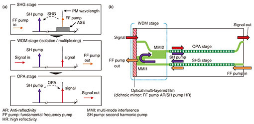
1. IntroductionOptical transmission reach and channel capacity will ultimately be limited by the degradation of the signal-to-noise ratio (SNR) resulting from nonlinear noise induced by the interplay between the Kerr effect in a fiber and amplified spontaneous emission (ASE) from optical amplifiers [1]. Phase-sensitive amplifiers (PSAs) are attracting much interest because they have the potential for low noise amplification while breaking the 3-dB quantum limit on the noise figure (NF) of conventional phase-insensitive amplifiers [2] and for signal regeneration capability [3]. These features mean that a PSA will be a promising candidate for solving the problem of transmission noise. PSAs based on χ(3) and χ(2) nonlinear processes can be implemented with different gain media (e.g. highly nonlinear optical fiber [4] or periodically poled lithium niobate (PPLN) [5]). We have used a PPLN waveguide as the gain medium in a χ(2)-based PSA. Recent advances in PPLN waveguides and related module packaging technology have enabled us to construct a χ(2)-based PSA for optical communication [6]. Using this PPLN-based PSA, we have successfully demonstrated a phase-sensitive amplification of polarization division multiplexing and wavelength division multiplexing signals with a practical gain of over 20 dB. However, such a highly functional PSA requires not only multiple PPLN waveguides but also many linear devices, such as beam combiners, polarization beam splitters, and delay or phase adjusters. The monolithic integration of PPLN waveguides is a promising approach for the practical use of a functional PSA with highly stable operation. In this article, we introduce our recent work on PPLN-waveguide-based monolithic-integration techniques for high-performance PSAs. This article is organized as follows. In section 2, we describe a single-chip integration of two PPLN waveguides and a wavelength-division multiplexer (WDM) that are basic components of the PPLN-based PSA. We then discuss the design and fabrication of this integrated device and demonstration of a continuous wave (CW)-pumped phase-sensitive parametric amplification using the device [7]. In section 3, we introduce a PSA using a high-power-tolerant electro-optic (EO) phase-modulator-integrated PPLN (PM-PPLN) waveguide. The PM-PPLN waveguide improves the SNR of the pump light and exhibits low-noise phase-sensitive amplification [8]. 2. Monolithically integrated parallel PPLN waveguides with reflective WDMThe basic structure of a PPLN-based PSA generally consists of three stages, namely a second harmonic generation (SHG) stage, WDM stage, and optical parametric amplification (OPA) stage. The process flow is shown schematically in Fig. 1(a). First, in the SHG stage, a strong fundamental frequency (FF) pump amplified using an optical amplifier, such as an erbium-doped fiber amplifier (EDFA), is used to generate a high-power second harmonic (SH) pump. Next, in the WDM stage, the SH pump and FF pump, which accompanies the ASE noise from the amplifier, are separated, and the SH pump is multiplexed with the signal. Finally, in the OPA stage, the signal and SH pump complete the parametric interaction. Kanter et al. successfully demonstrated squeezing in a PPLN-integrated optical waveguide circuit based on an annealed proton exchange waveguide [9]. This was the first report of a single-chip device in which two PPLN waveguides and a WDM are integrated. In this circuit, the basic components of an SH-pumped parametric amplifier consisting of two PPLN waveguides and a WDM were connected in tandem in the longitudinal direction. This configuration limits the conversion efficiency because such efficiency of a PPLN waveguide is proportional to the square of the waveguide length. To develop an integrated device with a high conversion efficiency, we designed a device structure in which two PPLN waveguides are arranged in parallel, which enables us to use the entire length of the wafer for each PPLN waveguide except for the multiplexing region. There are certain difficulties to overcome if we are to achieve parallel configuration. It is difficult for the WDM to connect two waveguides because they are densely configured. Moreover, the WDM must perform low-loss multiplexing and high isolation of the FF pump. This is because the coupling losses of the signal directly degrade the SNR, and, if the FF-pump isolation is insufficient, the FF-pump leakage and the accompanying ASE noise interfere with the signal, which degrades the quality of the output signal. Figure 1(b) shows a schematic of the integrated device. The parallel configuration of the two PPLN waveguides for SHG and OPA provide a long interaction length, and the reflection configuration of the WDM makes it possible to connect parallel waveguides that are configured densely. To achieve the high isolation of the FF pump and low loss coupling of the signal, the multi-mode interference (MMI) (de)multiplexers and dichroic mirror are integrated. We designed MMIs that exhibit straight coupling for a wavelength of 1.56 μm and cross coupling for a wavelength of 0.78 μm [10]. MMI1 is cut at around the center of the MMI length, and the cut surface is coated with dielectric multilayered film that functions as a dichroic mirror. The dichroic mirror has high reflectivity at the SH-pump wavelength (at 0.78 μm) and very low reflectivity at the FF-pump wavelength (at 1.56 μm). The SH pump is generated by SHG from a strong FF pump, which accompanies the ASE from the amplifier. In MMI1, the FF pump with ASE is filtered out from the edge of the chip, and only the SH pump reflects back to the cross port while the residual FF pump reflected from the chip edge re-enters the PPLN waveguide for SHG. The SH pump from the cross (input) port and the signal from the bar (input) port are multiplexed in MMI2, where the residual FF pump can again be filtered out. The signal and ASE-suppressed SH pump are then injected into the PPLN waveguide for OPA to achieve wavelength conversion.
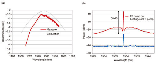
We prepared a Zn (zinc)-doped LN wafer for the waveguide core layer and a Mg (magnesium)-doped LN wafer for the substrate. The two wafers were directly bonded and a ridge waveguide was fabricated by dry etching [11]. We then deposited a dielectric multilayer on the end-face of the MMI1. To evaluate the excess losses of the MMI, we placed a straight waveguide along it as a reference. The PPLN section is 38-mm long, and the WDM section is 12-mm long giving a total device length of 50 mm. The fabricated waveguide thickness and width are 7 and 10 μm, respectively. Figure 2(a) shows the normalized transmittance of MMI2 as a function of input wavelength at the 1.5-μm band. We obtained a low excess loss of about 0.5 dB, which is close to the theoretical value of 0.1 dB. To estimate the isolation of the integrated WDM, we measured the leakage of the FF pump and FF pump out, which is the FF pump that passed through the edge of MMI1. Figure 2(b) shows the measured spectra. The red line is the spectrum for the FF pump out and the blue is for leakage of the FF pump. The difference between the peak for the FF pump out and that for the leakage of the FF pump shows the isolation to be as good as 60 dB. This means that two MMIs and a dichroic mirror sufficiently suppress the fundamental.
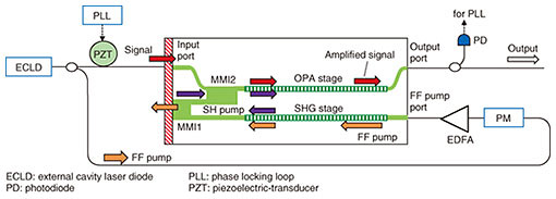
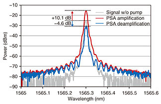
Figure 3 shows the experimental setup for degenerate phase-sensitive amplification using the integrated device. The signal and FF pump at 1562 nm were generated using an external cavity laser (ECL) for degenerate parametric processes. To achieve a stable PSA output, a phase-locking scheme in which a PM is used for phase dithering and a piezoelectric-transducer (PZT)-based optical phase locking loop (PLL) is used to compensate for the slow relative phase drifts between the signal and SH pump caused by thermal or acoustic vibrations. Both in-phase (amplification) and quadrature-phase (deamplification) condition of the relative phase between the signal and SH pump lights were obtainable individually by changing the setting of the PLL. Figure 4 shows the in-phase and quadrature-phase PSA output spectra for the signal. For the in-phase setting, an amplification of +10.1 dB was obtained, while a deamplification of –4.6 dB was obtained for the quadrature-phase setting. The amplification and deamplification gains are defined as the signal output divided by the signal output without pump injection. These results clearly indicate phase sensitivity. We successfully demonstrated a degenerate PSA with a CW pump using the integrated device.
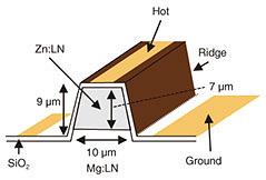
3. EO PM integrated SH-pump generator for low-noise amplificationA high SNR of the pump light is essential for achieving a low NF because the intensity noise of the pump is transferred to that of the amplified signal. The pump generator of χ(2)-based PSAs consists of an EDFA to boost the FF pump and SH generator of an FF pump. It also uses a phase-locking scheme, in which a PM is used for phase dithering and a PZT-based PLL to compensate for the slow relative phase drift between the signal and pump. To obtain both high-speed dithering and low-loss connectivity to other fiber pigtail components, a Ti (titanium)-diffused LN waveguide modulator has been used in χ(2)-based PSAs. Because of the low tolerance against the input power of a Ti-diffused LN waveguide due to photorefractive damage, the waveguide must be placed before the booster EDFA for pump generation. This decreases the input power to the EDFA, which results in the degradation in the SNR of the FF pump. To improve the SNR of the pump of a χ(2)-based PSA, we fabricated a high-power-tolerant EO PM-PPLN-based SH-pump generator. We used a directly bonded wafer consisting of Z-cut ZnO (zinc oxide)-doped LN as a core and MgO (magnesium oxide)-doped LN as a cladding layer, and a ridge structure was formed by dry etching. Next, we covered the ridges with an SiO2 (silicon dioxide) buffer layer to prevent any waveguide propagation loss from being induced by the electrodes of the PM. We then evaporated an Au (gold) thin film over the buffer layer and patterned the film into lumped-constant electrodes with a wet-etching process. Figure 5 is a schematic cross-section of the EO PM of the SH-pump generator. We formed a hot electrode on top of the ridge and two ground electrodes on the etched surface. With this structure, we were able to obtain a large index change with a vertical electric field. The lengths of the PPLN and PM regions were 37 and 18 mm, respectively, and the total length of the PM-PPLN waveguide was 55 mm. Finally, the PM-PPLN waveguide was packaged in a fiber pigtailed module using lens coupling without an optical adhesive. We also installed a dichromatic mirror in the module to filter the SH pump.
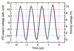
We measured the response of the output power from a modified crossed-Nicol setup to evaluate the phase-modulation characteristics. Figure 6 shows how the output power changed when the integrated EO PM was driven with a sinusoidal voltage at a frequency of 1 MHz. We clearly observed a phase modulation at 1 MHz, which is sufficient for the phase dithering of the PLL. We also confirmed the 3-dB bandwidth of the modulator exhibited over 10 MHz, which is sufficient for phase dithering.
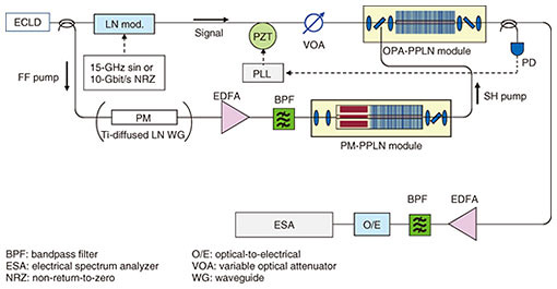
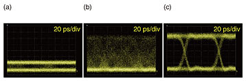
We then evaluated the potential of the PM-PPLN module in a PSA configuration. Figure 7 shows the experimental setup for this PSA. The FF pump was tapped from the signal and input into the SH-pump generator using the PM-PPLN module. The SH-pump light was injected into the other PPLN module for OPA. The signal was modulated using a Mach–Zehnder (MZ) LN modulator with a 10-Gbit/s non-return-to-zero (NRZ) format, attenuated with a variable optical attenuator (VOA), and injected into the OPA-PPLN module. The input power was monitored with a power meter. To maintain a stable PSA output, EO phase dithering in the PM-PPLN module was used for phase locking, and a PZT-based optical PLL was used to compensate for the relative phase difference between the signal and SH pump caused by thermal or acoustic vibrations. The output was tapped with a coupler, detected with a photodiode, and input into the PLL circuit. We observed the PSA output with a sampling oscilloscope to confirm the phase-locking operation. Figure 8 shows eye diagrams of the signal and output. Without phase dithering in the PM-PPLN module, although parametric amplification could be observed, the eye did not open because of fluctuations in the relative phase between the signal and SH pump, as shown in Fig. 8(b). With phase dithering at 1 MHz, the eye was clearly open, as shown in Fig. 8(c).
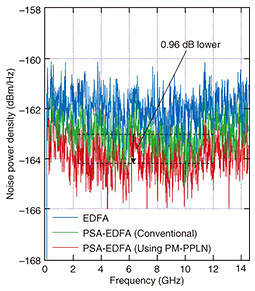
We examined the effect of improving the SNR of the pump light by evaluating the noise characteristics of a conventional PSA and a PSA using the PM-PPLN module. In the conventional PSA, we used a commercially available Ti-LN PM placed before the EDFA with an insertion loss of 5.5 dB. We generated an SH pump with the same PM-PPLN module. To evaluate the NF properties, we captured the noise components in the 1- to 14-GHz range with an electrical spectrum analyzer (ESA) [12]. We cascaded the PSA with an EDFA to mitigate the narrow dynamic range of the ESA. The signal was modulated using a chirp-less MZ modulator with a 15-GHz sinusoidal wave. The gain of the amplifiers was measured using the intensity at the modulation frequency of 15 GHz. We measured the output-noise power densities for the PSA using the PM-PPLN module and EDFA cascaded amplifier, for the conventional PSA and EDFA cascaded amplifier, and for a stand-alone EDFA used for a reference. Figure 9 shows electrical noise spectra in the 1- to 14-GHz range for all the amplifiers under the same input signal-power condition of −28 dBm. The dashed straight lines in Fig. 9 show the average noise-power densities for the PSA using the PM-PPLN module and EDFA cascaded amplifier and for the conventional PSA and EDFA cascaded amplifier in the 2- to 12-GHz region. In all cases, the total gain of the PSAs and the cascaded EDFA were about 17.5 dB, as was the gain of the stand-alone EDFA. The cascaded amplifiers exhibited a lower noise level than the stand-alone EDFA over the entire frequency range. Specifically, the noise power was 0.96 dB lower for the PSA using the PM-PPLN module and EDFA cascaded amplifier than for the conventional PSA and EDFA cascaded amplifier. We then calculated the NF values of both PSAs by using the noise level of the stand-alone EDFA and gain values of the PSAs and cascaded EDFA and NF of the cascaded EDFA [12]. Under an input-power condition of −28 dBm and gain condition of 17.5 dB, the measured NF of the stand-alone EDFA used for the reference was about 5.35 dB. In contrast, the PSAs exhibited lower NFs. The calculated NFs of the conventional PSA and the PSA using the PM-PPLN module were about 3.09 and 2.22 dB, respectively. We confirmed that the SNR of the PSA using the PM-PPLN module improved by comparing the NF of the conventional PSA using a Ti-LN PM.
4. SummaryWe introduced our recent results for PPLN-waveguide-based monolithically integrated devices for PSAs. We described the design and fabrication of the device that integrates two-stage SHG and OPA processes on one chip. We successfully demonstrated a CW-pumped PSA using this integrated device with an amplification gain of over 10 dB. A PM-integrated PPLN SH generator was also shown to improve the SNR of the pump light for the PSA. Using the PM-PPLN module as a pump source for a PSA, we confirmed low-noise phase-sensitive amplification. We believe that the integration of functional devices will be key to achieving a high-performance PSA that can extend the capacity of optical communication networks. References
|
||||||||||||||||||||||||||