|
|||||||
|
|
|||||||
|
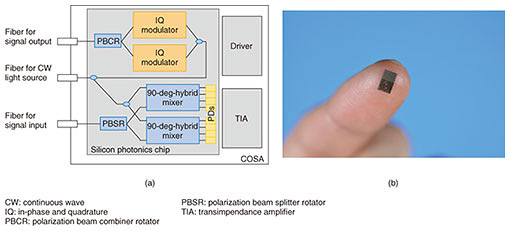
Feature Articles: Photonics-electronics Convergence Technology to Achieve All-Photonics Network Vol. 18, No. 10, pp. 16–20, Oct. 2020. https://doi.org/10.53829/ntr202010fa2 Ultracompact Silicon Photonics Coherent Optical Subassembly for Ultrahigh-capacity Optical CommunicationAbstractToward the All-Photonics Network, which is a key element of the Innovative Optical and Wireless Network (IOWN), we at NTT Device Innovation Center are developing an ultracompact optical transceiver module as a photonics-electronics convergence device. By using silicon photonics technology and co-packaging electronic devices, we fabricated an ultracompact coherent optical module for next high-capacity optical networks. Keywords: silicon photonics, digital coherent, coherent optical subassembly (COSA)  1. IntroductionAlong with the diversification of communication services, the data traffic that should be processed by information technology (IT) systems in a network has increased dramatically, and the amount of power consumed by IT systems has increased. Therefore, NTT proposed a network concept called the Innovative Optical and Wireless Network (IOWN) to manage the ever-growing traffic and provide a communication network with even greater capacity, lower latency, lower power consumption, and flexibility. The All Photonics Network (APN), one of the key elements of IOWN, introduces photonics everywhere in a communication network. By applying photonics for shorter distance transmission than current networks, the APN is aimed at achieving low power consumption, and high-quality, large-capacity, and low-latency transmission. To adopt photonics to shorter distance transmission, it is necessary to dramatically reduce the size as well as cost of photonics devices. Photonics-electronics convergence technology [1] is a key enabler for such improvement. At NTT Device Innovation Center, we are developing optical transceiver modules using silicon photonics technology to not only minimize optical interfaces for high-speed transmission but also to reduce power consumption. By integrating an optical circuit into a single silicon chip and co-packaging this with an analog electronic circuit, we developed an ultracompact coherent module for digital coherent transceivers. We call this module coherent optical subassembly (COSA). This integration is a photonics-electronics convergence technology and can significantly reduce the size and cost of the optical interface in a network. 2. Silicon photonics technologySince the early 2000s, NTT Science and Core Technology Laboratory Group has been working on silicon photonics technology and is a pioneer in this field. Silicon photonics technology uses transparent silicon in the communication wavelength band (1.3 to 1.5 μm) as a platform for optical integrated circuits (ICs) by using the fabrication technology developed for large-scale integrated circuits. Silicon photonics technology enables the mounting of not only simple optical passive elements but also optical active components, including optical modulators and germanium photodetectors (PDs), on silicon. Optical devices in optical transceivers have traditionally been fabricated using different material systems. These conventional discrete devices are interconnected using optical fibers and spatial optics. NTT has succeeded in developing key optical devices by using silicon photonics technology and integrating them on a single silicon chip. By mounting such a silicon photonics chip together with an electronic circuit in the same package, a compact optical module for an optical transceiver can be fabricated. 3. COSA for digital coherent transmissionDigital coherent transmission can compensate for the various optical signal distortions received during optical transmission due to its powerful electrical compensation technology and has been developed for long-distance transmission from hundreds to thousands of kilometers. We are currently studying the application of such digital coherent transmission technology even for short-distance applications such as intra- and/or inter-datacenter communication where the traffic has increased remarkably during the last decade. The Optical Internetworking Forum (OIF), which is an industrial association promoting network solutions through the creation of Implementation Agreements, defines standards for power consumption and the size of digital coherent optical transceivers. OIF has set a new standard for digital coherent optical transceivers every one to two years since 2012 and demands smaller sizes each time. Around 2012, the standardized size of a transceiver was 12.7 × 17.8 cm, but a smaller size of 2 × 8 cm is currently required. Such a small form factor is called quad small form factor pluggable-double density. At the same time, standard transmission speed also increased from 100 to 400 Gbit/s. Expanding traffic related to datacenter networks mainly drove such demand for reducing the size and increasing bandwidth. Therefore, NTT argued that silicon photonics technology can be used for digital coherent optical transceivers [2]. A conceptual diagram of COSA is shown in Fig. 1(a). A silicon photonics chip, transimpedance amplifier that converts the output current of the receiving PD into a voltage signal, and driver that drives the optical modulator are integrated in one package. In the silicon photonics chip, an in-phase and quadrature modulator and polarization beam combiner rotor is integrated on the transmitter side. On the receiver side, a polarization beam splitter, 90-degree optical mixer, and high-speed PD array are integrated. On both transmitter and receiver sides, a PD for monitoring the optical signal power of transmission and reception is also integrated. In a conventional coherent transceiver, these optical elements are separate devices using different material systems and are interconnected by optical fibers, optical lenses and so on. Therefore, there is a limit to reducing the size of the transceiver. COSA integrates these key optical devices on a single chip, so dramatic size reduction can be achieved, as shown in Fig. 1(b). This chip was mounted in a package together with drivers and electronic devices as COSA for 400-Gbit/s transmission.
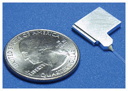
We also removed the temperature control units, which are often used in conventional optical components, to reduce the module size. This is the result of the temperature-independence design of the circuits in a silicon photonics chip. The humidity-tolerant design of each chip in COSA also enables us to reduce the module size because we can use a non-hermetic package, which is smaller than the conventional hermetic package. The optical coupling structure based on the directly attached fiber on the silicon edge also contributed to downsizing the device footprint and height. Figure 2 is a photograph of COSA. COSA is currently available in a very small and thin package of 19 × 12 × 2.1 mm. Now that the miniaturization of digital coherent optical transceivers is progressing, further miniaturization is expected to accelerate by applying COSA.
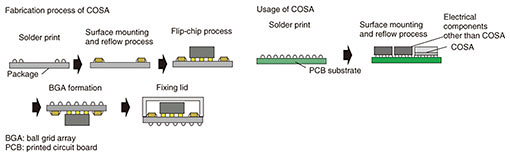
Figure 3 shows the conceptual diagram of the assembly process of COSA. After mounting the components on the package by solder printing and reflow, the chips are mounted. After that, a ball grid array, which is an input/output interface for high-speed electrical and control signals and power supply, is formed. The lid and fibers are then fixed. In this process, full automation of mounting is achieved, contributing to COSA’s high productivity and economic efficiency. When mounting on a printed circuit board of an optical transceiver, COSA can be mounted through an automatic surface mount technology (SMT) process together with other electronic components. Most conventional optical devices require individual mounting processes after an SMT process of electronic components. Therefore, COSA can make the assembly process of a transceiver significantly easier and faster.
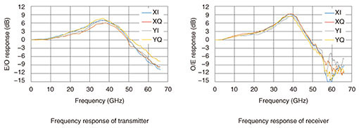
4. Next challengeThe APN is a key component of IOWN for introducing photonics everywhere in a communication network. To apply photonics to shorter-distance transmission and even to chip interconnection between an electronic processer, it is necessary to make optical transceiver modules smaller and faster. Currently, only a few analog electronic chips can be integrated in the package of COSA, but larger scale co-packaging will be necessary in the future. It is also required to increase the data rate of the signal transmission. To further develop and expand photonics-electronics convergence technology, NTT Device Innovation Center is conducting R&D for significantly improving transmission speed of COSA. Compared to 400-Gbit/s transmission, which supports 64-Gbaud signal, we successfully expanded the capable signal baudrate to 100 Gbaud [3]. By expanding the electrical-to-optical (E/O) and optical-to-electrical (O/E) bandwidth of COSA, we significantly improved transmission speed. Figure 4 shows the improved E/O and O/E bandwidth of the 100-Gbaud class COSA. By improving not only the silicon photonics chip but also the co-packaging technology, the 3-dB bandwidth of the O/E and E/O responses was improved to about 50 GHz.
We confirmed that COSA is a key technology for future ultrahigh-capacity optical networks and that silicon photonics technology will be key for photonics-electronics convergence technology. References
|
|||||||